

Semiconductor device and method for fabricating the same
a semiconductor and device technology, applied in semiconductor devices, digital storage, instruments, etc., can solve the problems of fluctuation of the characteristics of the transistor and weaken the effect of reducing the stress that is the original purpose of the approach, and achieve the effect of lowering the processing temperature for forming
- Summary
- Abstract
- Description
- Claims
- Application Information
AI Technical Summary
Benefits of technology
Problems solved by technology
Method used
Image

Examples
first embodiment
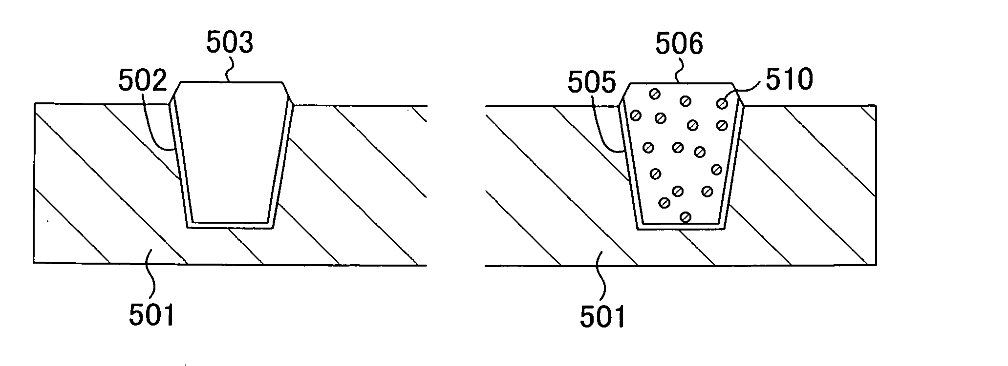
[0038]FIG. 1 is a sectional view showing an STI portion (isolation region) of a semiconductor device according to a first embodiment of the present invention. The semiconductor device of the first embodiment includes: a silicon substrate (semiconductor substrate) 101 formed with an active region and an isolation region surrounding the active region; and a transistor (not shown) such as a MIS transistor provided on the active region of the silicon substrate 101. The isolation region of the silicon substrate 101 is formed with a trench which has a width of about 0.1 μm and a depth of about 0.2 μm and of which an inner wall is covered with a side wall oxide film 102. The inside of this trench is filled with an insulating film 103 for isolation (an isolation insulating film 103) made of silicon oxide, and silicon nanocrystals (semiconductor microparticles) 105 with a diameter of about 5 nm are buried in the isolation insulating film 103.
[0039] In the first embodiment, the volume fillin...
second embodiment
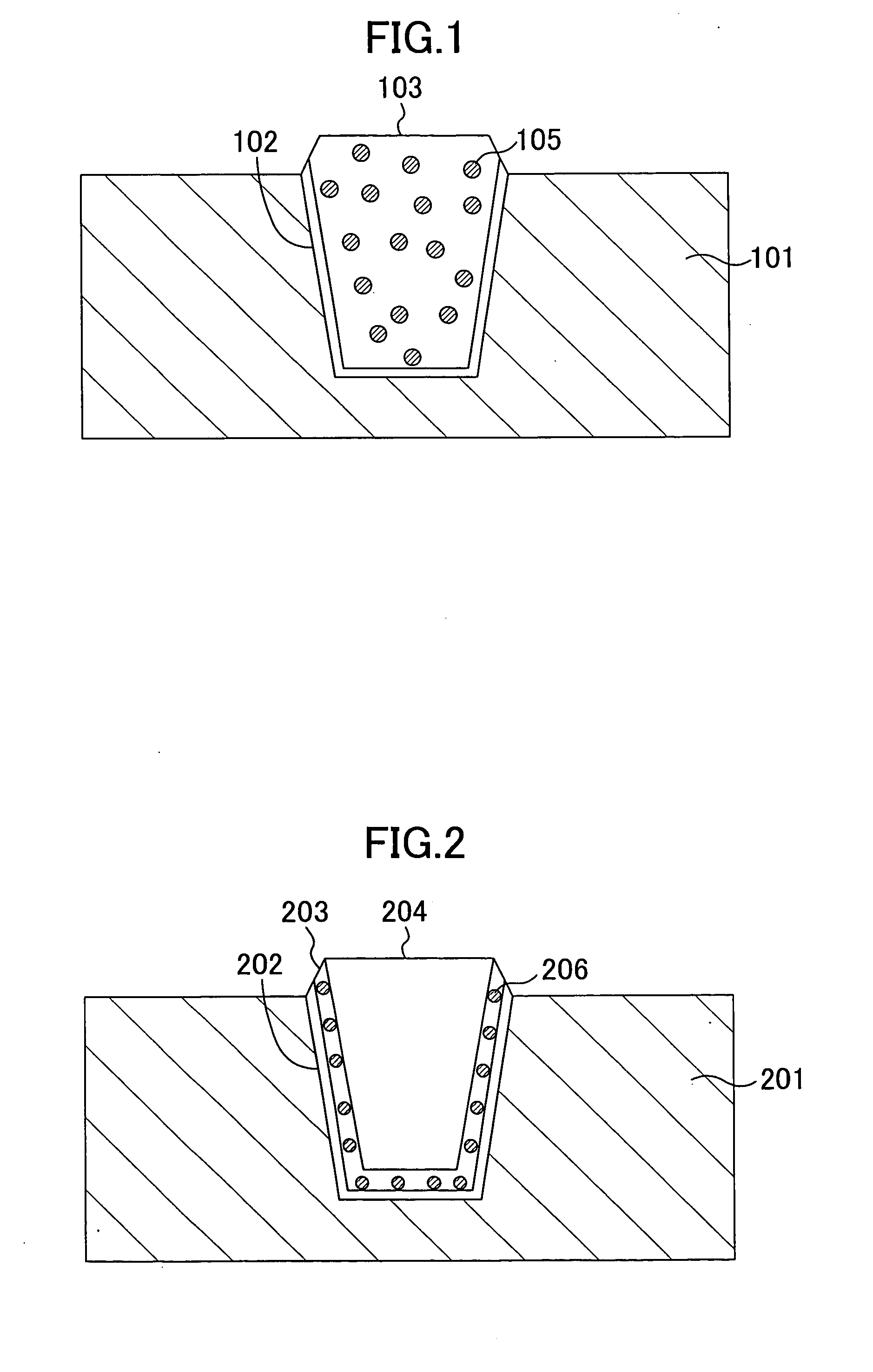
[0052]FIG. 2 is a sectional view showing an STI portion of a semiconductor device according to a second embodiment of the present invention.
[0053] In the semiconductor device of the first embodiment, the silicon nanocrystals 105 (see FIG. 1) disperse uniformly in the entire isolation insulating film 103. On the other hand, in the semiconductor device of the second embodiment, silicon nanocrystals 206 are provided only within a liner layer (first insulating film) 203 of silicon oxide having a thickness of about 20 nm and covering a side wall oxide film 202 inside a trench. The lower limit of the distance between the silicon nanocrystals 206 is set at about 1.5 nm or more. The isolation insulating film (second insulating film) 204 of silicon oxide formed on the liner layer 203 fills the trench formed in the silicon substrate 201. Note that the trench formed in the STI portion has a width of, for example, about 0.1 μm, and the isolation insulating film 204 has a width of about 0.04 μm...
third embodiment
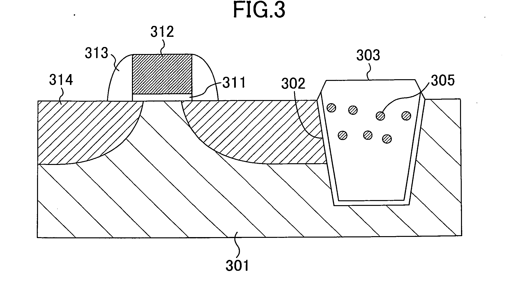
[0061]FIG. 3 is a sectional view showing a semiconductor device according to a third embodiment of the present invention. Referring to FIG. 3, the semiconductor device of the third embodiment includes: a lateral transistor in which carriers flow in the parallel direction to a substrate surface; and an isolation insulating film formed in an isolation region. FIG. 3 shows an exemplary case where a MOS (MIS) transistor is provided as the lateral transistor.
[0062] To be more specific, the semiconductor device of the third embodiment includes: a silicon substrate 301 formed with an active region and an isolation region surrounding the active region; and a transistor (not shown) such as a MOS transistor provided on an active region of the silicon substrate 301.
[0063] The MOS transistor includes: a gate insulating film 311 of a silicon oxide film or the like provided on a silicon substrate 301; a gate electrode 312 provided on the gate insulating film 311; impurity diffusion regions 314 ...
PUM
 Abstract
Description
Claims
Application Information