Optical devices featuring textured semiconductor layers

a technology of optical devices and semiconductor layers, applied in the direction of semiconductor devices, electrical devices, nanotechnology, etc., can solve the problems of slow index-material degradation, low efficiency of internal efficiency, and some manufacturing limitations, so as to improve the efficiency of light extraction and coupling light into the device, and enhance light escape

Active Publication Date: 2007-05-31
TRUSTEES OF BOSTON UNIV
View PDF58 Cites 291 Cited by
  • Summary
  • Abstract
  • Description
  • Claims
  • Application Information

AI Technical Summary

Benefits of technology

[0009] The present invention provides a device for use as a light emitter or sensor or as a solar cell. For an emitter of the invention based on polar semiconductors such as III-nitrides, the IQE and light extraction efficiency is improved over conventional devices. For a sensor or solar cell, the efficiency of coupling light into the device is also improved. In one embodiment, the semiconductor material is deposited in layers, starting with as grown textured initial semiconductor layer deposited onto a substrate. In one embodiment, the layer is randomly textured as grown on the substrate so as to have a textured surface morphology. The substrate and textured layer can be used as a template for the growth of multiple semiconductor layers. For example, a device may comprise a second layer deposited onto the first textured layer. These layers can be deposited with p and n dopants to form a p-n junction LED. The textured emitting layer enhances light escape. The initial semiconductor layer preferably serves as a barrier layer onto which a quantum well layer is grown. Each of the semiconductor layers conforms to the texture of the first grown layer and thus the external surface of the LED from where the light is extracted has approximately the same texture as the initial semiconductor layer.

Problems solved by technology

In the case of nitride LEDs grown along polar (0001) and (000-1) directions the internal efficiency is also reduced due to the distortion of the quantum wells between the n- and p-doped layers caused by the internal electric fields.
Some of these approaches have some manufacturing limitations and the last one suffers from fast index-material degradation with time.

Method used


Image

  • Optical devices featuring textured semiconductor layers
  • Optical devices featuring textured semiconductor layers
  • Optical devices featuring textured semiconductor layers

Examples


example i

Growth of Textured GaN Templates by HVPE

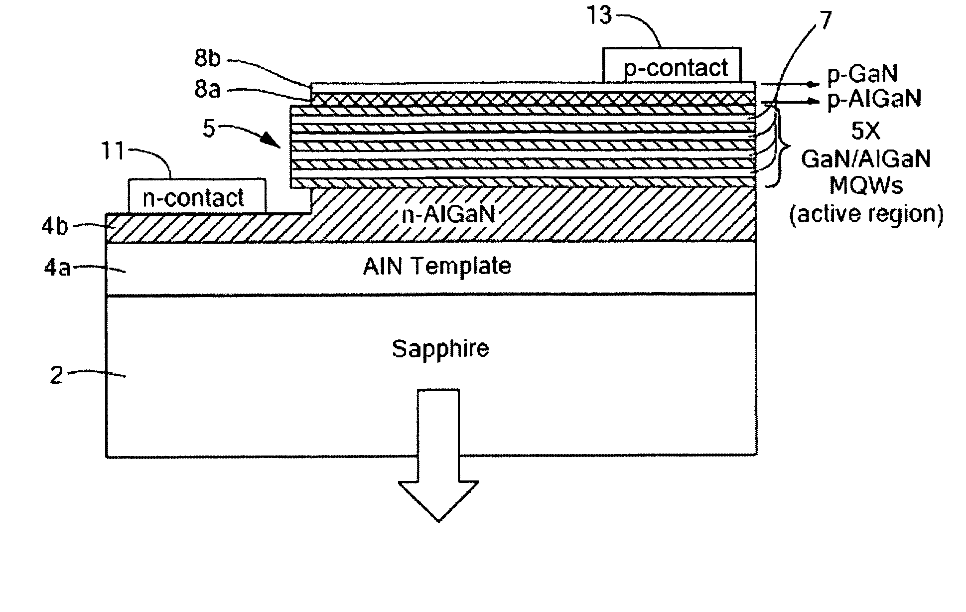
[0129] Textured GaN templates were fabricated by the modified HVPE process described above. FIG. 7 shows an electrically excited wafer level LED radiating at p contact 20. This blue LED structure was made on an unpolished (0001) sapphire substrate. On this substrate was grown 3 microns of heavily doped n-type GaN, followed by 10 MQWs consisting of InGaN with 13% indium as the wells and GaN as the barriers. The growth of the MQWs is followed by a thin (about 10 nm) electron blocking layer consisting of AlGaN with 30% Al doped p-type with magnesium, and this is followed by 200 nm of heavily p-type doped GaN with magnesium. The free surface from where the light is emitted has replicated the morphology of the unpolished sapphire substrate.

[0130]FIG. 8a shows a scanning electron microscope (SEM) image of a GaN template randomly textured as grown via the modified HVPE process. The image was captured with the sample tilted about thirty degrees with...

example ii

Growth of Multiple Wrinkled Quantum Wells on a Textured Template

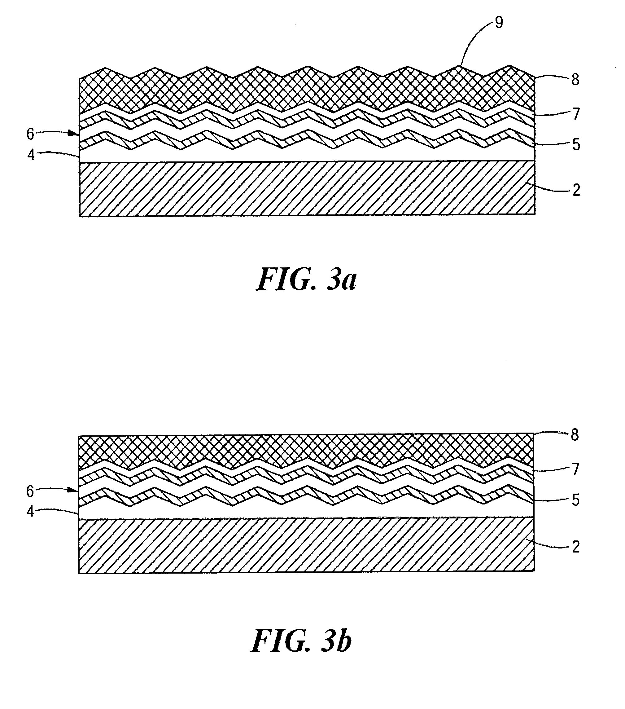
[0134]FIG. 6 is a transmission electron microscope image showing multiple quantum wells on a textured surface (wrinkled quantum wells). The quantum wells comprise ten pairs of AlGaN and GaN layers. An individual GaN layer may comprise a textured quantum well layer with the AlGaN layer serving as the barrier layer. The composition of the AlGaN layer, for example, is Al0.2Ga0.8N. Generally, that is AlxGa1-xN. The multiple quantum wells can also be made by any combination of small gap III-V nitride films (wells) and large gap III-V nitride films (barriers). The composition of the MQW determines the emission energy of light from about 0.7 eV of pure InN to 6 eV from pure AlN. The plurality of quantum well layers are grown by any suitable deposition process. A MBE process involves the reaction of a group III material with nitrogen that has been activated by radio frequency or microwave plasma. An alternative approach would ...

example iii

Textured Surface Made by Etching of a Masked Template

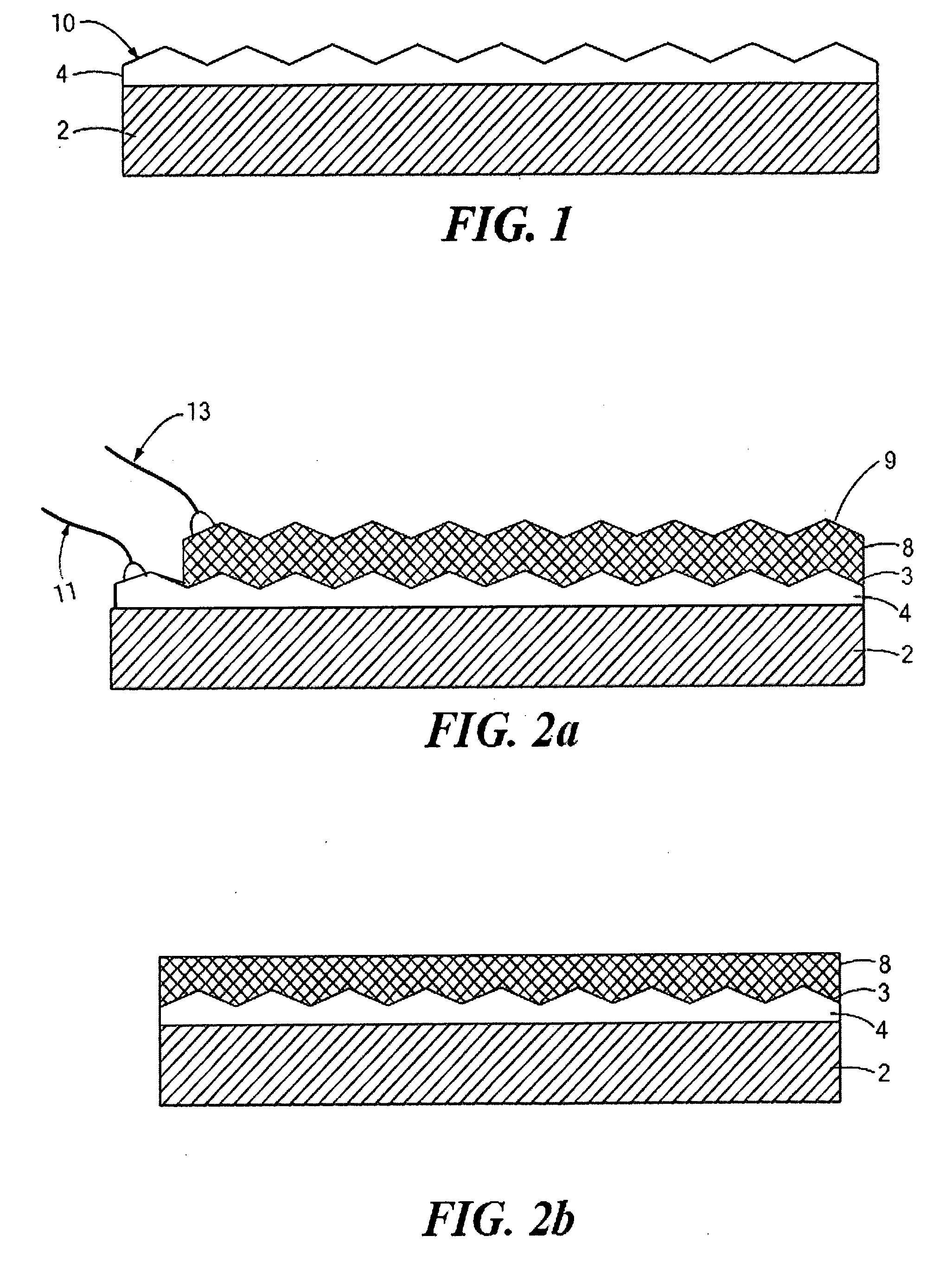
[0141] In this example, a textured substrate is created with a textured surface on which additional layers are grown, while replicating the textured features. The additional layers may be grown so as to form a textured template, a p-n junction or an optical device of the invention. The additional layer(s) may also comprise multiple quantum wells formed by a plurality of well and barrier layers. The surface of the substrate to be textured may be smooth or previously textured. The surface of the substrate can also be unaltered or otherwise natural.

[0142] A mask structure comprising a monolayer of monodisperse spherical colloidal particles is coated onto the surface of the substrate. The substrate can include silicon, silicon carbide, sapphire, gallium arsenide, gallium nitride, aluminum nitride, zinc oxide, or glass. Spherical monodisperse colloidal particles can be commercially obtained in sizes ranging from 0.02 to 10 microns. T...


PUM


Abstract

A semiconductor sensor, solar cell or emitter, or a precursor therefor, has a substrate and one or more textured semiconductor layers deposited onto the substrate. The textured layers enhance light extraction or absorption. Texturing in the region of multiple quantum wells greatly enhances internal quantum efficiency if the semiconductor is polar and the quantum wells are grown along the polar direction. Electroluminescence of LEDs of the invention is dichromatic, and results in variable color LEDs, including white LEDs, without the use of phosphor.

Description

CROSS REFERENCE TO RELATED APPLICATIONS [0001] This application claims the priority of U.S. Provisional Application No. 60 / 732,034 filed Oct. 31, 2005 and entitled, OPTICAL DEVICES FEATURING TEXTURED SEMMICONDUCTOR LAYERS. This application is also a continuation-in-part of pending U.S. application Ser. No. 11 / 107,150 filed Apr. 15, 2005 and entitled OPTICAL DEVICES FEATURING TEXTURED SEMICONDUCTOR LAYERS, which claims the priority of U.S. Provisional Application No. 60 / 562,489 filed Apr. 15, 2004 and entitled, FORMATION OF TEXTURED III-NITRIDE TEMPLATES FOR THE FABRICATION OF EFFICIENT OPTICAL DEVICES, U.S. Provisional Application No. 60 / 615,047 filed Oct. 1, 2004 and entitled, FORMATION OF TEXTURED III-NITRIDE TEMPLATES FOR THE FABRICATION OF EFFICIENT OPTICAL DEVICES, and U.S. Provisional Application No. 60 / 645,704 filed Jan. 21, 2005 and entitled, NITRIDE LEDS BASED ON FLAT AND WRINKLED QUANTUM WELLS. Further, this application is a continuation-in-part of PCT / US / 2005 / 012849 filed...

Claims


Application Information

Patent Timeline
Patent Type & Authority Applications(United States)
IPC IPC(8): H01L33/00H01L33/06H01L33/22H01L33/24H01L33/32
CPCB82Y20/00H01L29/155H01L29/2003H01L31/0236H01L31/035236H01L31/035281H01L31/03529H01L31/184H01L31/1852H01L33/06H01L33/22H01L33/24H01L33/32Y02E10/544H01L31/02363
Inventor MOUSTAKAS, THEODORE D.CABALU, JASPER S.
Owner TRUSTEES OF BOSTON UNIV
Why Eureka
Try Eureka