Membrane structure and method of making

a membrane structure and membrane technology, applied in the field of membrane structures, can solve the problems of high flux, high selectivity, and difficult to get a defect-free interface between layers, and achieve the effect of high selectivity and high flux

Inactive Publication Date: 2007-06-07
GENERAL ELECTRIC CO
View PDF8 Cites 46 Cited by
  • Summary
  • Abstract
  • Description
  • Claims
  • Application Information

AI Technical Summary

Benefits of technology

[0004] The present invention meets these and other needs by providing a m

Problems solved by technology

Typically thin membranes with small pores are stacked on thicker substrates with coarser pores, which provide mechanical support but do not significantly increase the resistanc

Method used


Image

  • Membrane structure and method of making
  • Membrane structure and method of making
  • Membrane structure and method of making

Examples


example 1

Method for Fabricating a Membrane Structure of Anodized Alumina on a Porous Polyethersulphone Support Layer.

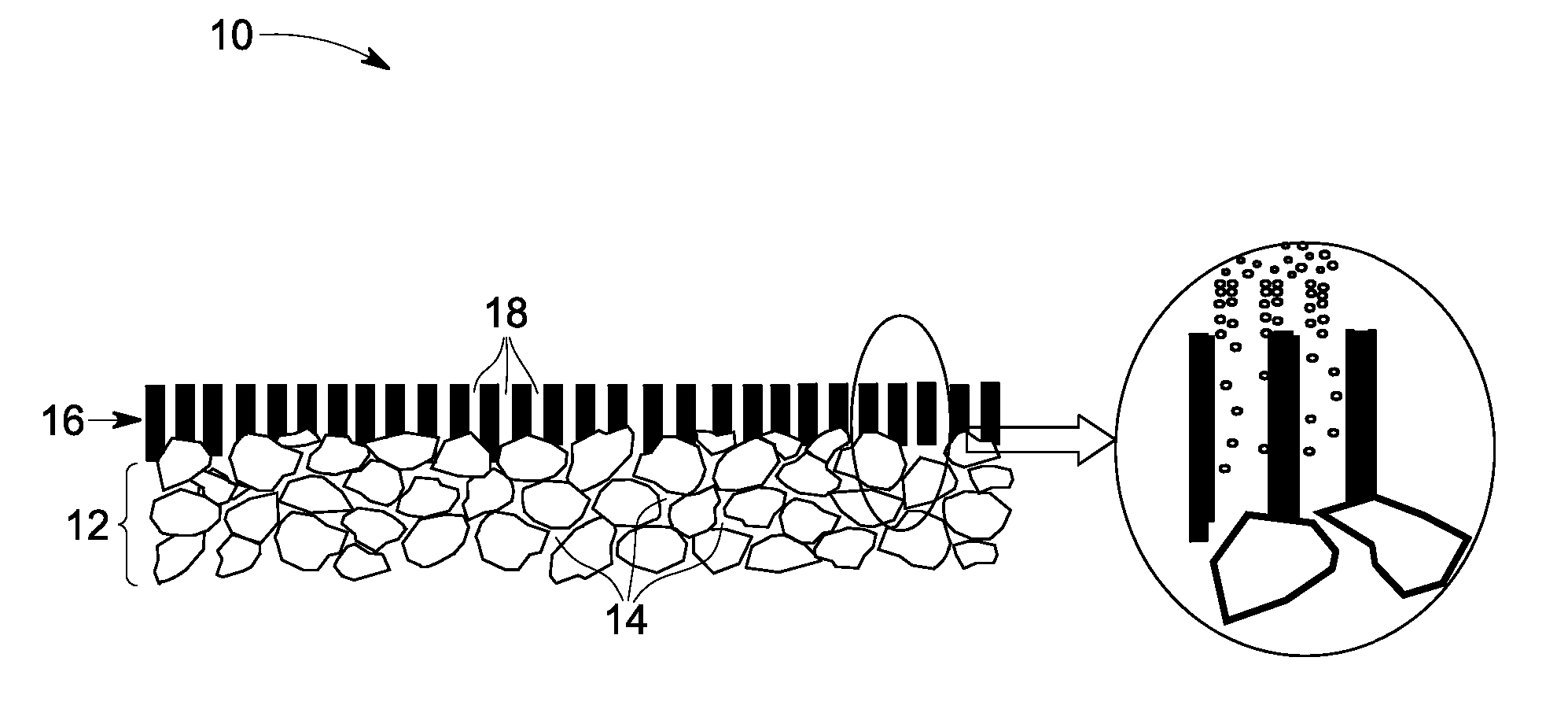
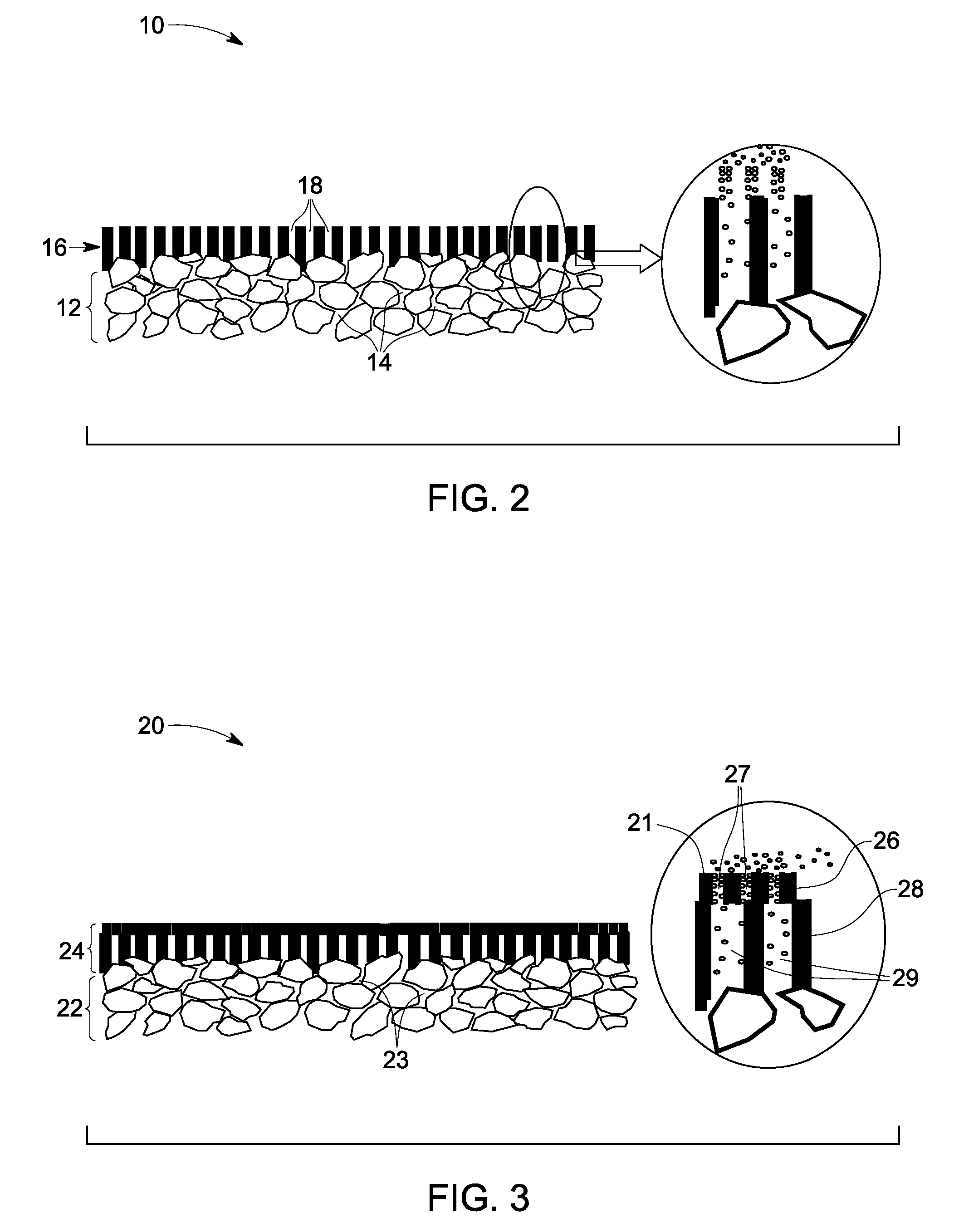
[0068] A continuous aluminum coating of thickness of about 1 micrometer was deposited on a porous polyethersulfone support. Polyethersulfone support layer has an average pore size of about 0.22 micrometers. The aluminum surface was masked with a lacquer mask and then anodized through the porous support. Anodization was done in 0.3 M oxalic acid at voltages greater than 20 V. The anodized alumina pore diameter was controlled, in large part, by the anodization voltage. The anodized alumina layer thickness was determined by anodization time. Once the anodized alumina layer was of the desired thickness, anodization was stopped. The polyethersulfone membrane was protected, the lacquer mask was dissolved with a suitable solvent, and the remaining unconverted aluminum was etched using a copper chloride solution. Finally, a barrier oxide layer was etched away using 5 wt % phosphoric...

example 2

Method for Fabricating a Embrane Structure of Asymmetric Anodized Alumina on a Porous Polyethersulfone Support Layer.

[0069] A continuous aluminum coating of thickness in the range of 1 micrometer to 2 micrometers was deposited, by evaporation, on a porous polyethersulfone support. The aluminum surface was masked with lacquer, and then anodized through the porous support. Anodization was conducted in oxalic acid at voltages greater than 20 V, as described above. Once the anodized alumina layer was of the desired thickness, anodization voltage is decreased to generate a porous sublayer with finer pores than those of the layer formed at 20V. Multiple alumina sublayers with decreasing pore size was fabricated by sequential reduction in anodization voltage. Any remaining aluminum was etched using a copper chloride solution. Finally, the barrier oxide layer was etched away using 5 wt % phosphoric acid to reveal the top surface of the porous alumina layer.


PUM

PropertyMeasurementUnit
Pore sizeaaaaaaaaaa
Pore sizeaaaaaaaaaa
Pore sizeaaaaaaaaaa

Abstract

A membrane structure is provided. The membrane structure includes a polymer layer having a plurality of pores; and a ceramic layer disposed on the polymer layer. The ceramic layer has a plurality of substantially unconnected pores. Each of the substantially unconnected pores is in fluid communication with at least one of the pores of the polymer layer. A method of manufacturing a membrane structure is provided. The method includes the steps of providing a polymer layer having a plurality of pores; and disposing a ceramic layer on the polymer layer. Disposing a ceramic layer includes depositing a metal layer on the polymer layer; and anodizing the metal layer to convert the metal layer into a porous layer. At least one of the depositing step and the anodizing step is performed as a continuous process. Alternatively, at least one of the depositing and the anodizing step is performed as a batch process.

Description

CROSS REFERENCE TO RELATED APPLICATIONS [0001] This application is a continuation-in-part of U.S. patent application Ser. No. 11 / 296,746, entitled “MEMBRANE STRUCTURE AND METHOD OF MAKING”, filed on Dec. 7, 2005, which is herein incorporated by reference.BACKGROUND [0002] The invention relates generally to membrane structures. More particularly, the invention relates to membrane structures having substantially high flux and substantially high selectivity. The invention also relates to a method of manufacturing membrane structures, on an industrial scale. [0003] Porous membrane structures are extensively used in filtration, separation, catalysis, detection, and sensor applications. Membrane structures with extremely fine pore sizes may be required for biofiltration and bioseparation applications. The selectivity of a membrane is typically determined by the membrane pore size—high selectivity membranes have small pores. However for a given thickness, the smaller the pore size, the sma...

Claims


Application Information

Patent Timeline
IPC IPC(8): B01D71/06
CPCB01D67/0062B01D69/12B01D71/022B01J2219/00835B01J2219/00907Y10T428/249981B01D69/1218B01D69/1213B01D69/1216B01D71/0221
Inventor RAMASWAMY, VIDYARUUD, JAMES ANTHONYKU, ANTHONY YU-CHUNGHUBER, WILLIAM HULLINGER
Owner GENERAL ELECTRIC CO
Why Eureka
Try Eureka