Nanocrystal and photovoltaic device comprising the same

a photovoltaic device and nano-crystalline technology, applied in the field of nano-crystalline materials, can solve the problems of long operating life of solar cells, high equipment cost, high manufacturing cost, etc., and achieve the effect of effectively converting light energy into electric energy and high light absorption efficiency

Inactive Publication Date: 2007-07-05
IND TECH RES INST
View PDF9 Cites 30 Cited by
  • Summary
  • Abstract
  • Description
  • Claims
  • Application Information

AI Technical Summary

Benefits of technology

[0012]The present invention provides a nanocrystal with high light absorption efficiency, and a photovoltaic device using the same. Consequently

Problems solved by technology

In addition, the solar cell has a long operating life-time.
However, it has the problems of high equipment cost and high manufacturing cost.
Even replacing the silicon semiconductor with other semiconductor materials, such as indium gallium nitride (InGaN), the issue of high cost still exists.
Hence, the application of solar cells is restricted in specific places, such as the space, remote districts, or exhibitions.
Furthermore, the popularity of solar cells among ordinary people is still low.
Unfortunately, the mobility of organic conjugated polymer (−4 cm2V−1s−1) is lower than that of the silicon semiconductor (>103 cm2V−1s−1).
As a result, the photoelectrical conversion efficien

Method used


Image

  • Nanocrystal and photovoltaic device comprising the same
  • Nanocrystal and photovoltaic device comprising the same
  • Nanocrystal and photovoltaic device comprising the same

Examples


embodiment 1

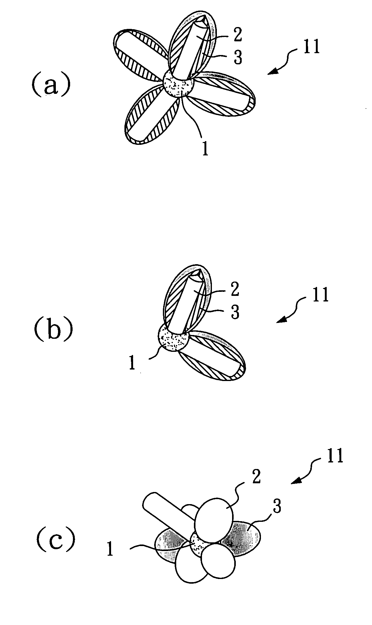
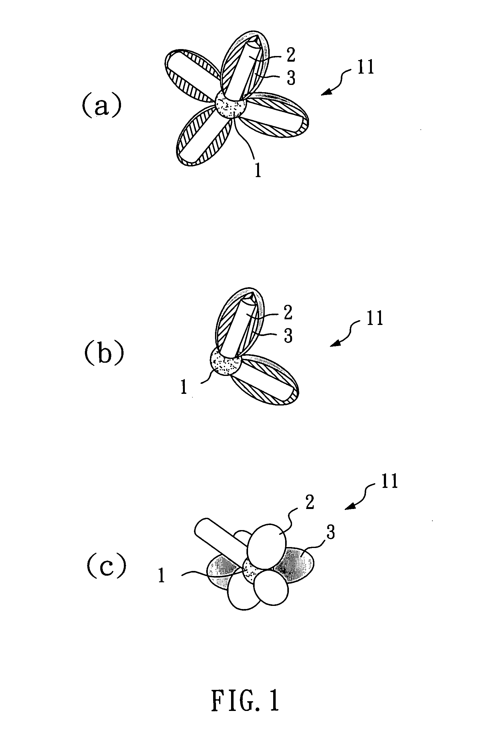
[0036]With reference to FIGS. 1a to 1c, schematic diagrams of a nanocrystal according to the preferred embodiments of the present invention are illustrated. As shown in FIGS. 1a to 1c, the nanocrystal comprises a core 1, a first shell 2, and a second shell 3. In this embodiment, the core 1 is composed of ZnSe semiconductor with a structure of a quantum dot, the first shell 2 is composed of a CdSe semiconductor, and the second shell 3 is composed of a PbSe inorganic material. Therefore, the nanocrystal 11 of this embodiment includes three materials with different absorption wavelengths. The wavelength of the absorption light of the ZnSe semiconductor is in the range of ultraviolet. The wavelength of the absorption light of the CdSe semiconductor is in the range of visible light. The wavelength of the absorption light of the PbSe inorganic material is in the range of infrared light.

[0037]As shown in FIG. 1a, the shape of the nanocrystal 11 is a tetrapod. The first shell is grown and f...

embodiment 2

[0046]FIGS. 3 to 5 shows photovoltaic devices 100, 200, and 300 according to the preferred embodiments of the present invention. As shown in FIGS. 3 to 5, the photovoltaic devices 100, 200, and 300 mainly comprise a photoactive layer having plural nanocrystals therein, a flexible top substrate 20, and a flexible bottom substrate, wherein the photoactive layer is disposed between the top substrate 20 and the bottom substrate 30.

[0047]In this embodiment, the photoactive layer contains 85 wt % of nanocrystals 11, and 15 wt % of Poly(3-hexylthiophene) (P3HT) as the organic conductive material. As shown in FIGS. 3 to 5, the top substrate 20 includes a substrate 21 and a first electrode 22. The bottom substrate 30 includes a substrate 31, a second electrode 32, and a carrier transfer layer 33. In this embodiment, the first electrode is a cathode composed of aluminum, the second electrode is an anode composed of indium-tin oxide, and the material of the carrier transfer layer 33 is a combi...


PUM

PropertyMeasurementUnit
Fractionaaaaaaaaaa
Fractionaaaaaaaaaa
Percent by massaaaaaaaaaa

Abstract

A nanocrystal with high light absorption efficiency and a broad absorption spectrum, and a photovoltaic device comprising the nanocrystal are disclosed. The nanocrystal of the present invention comprises a core, a first shell grown and formed on the surface of the core, and a second shell grown and formed on the surface of the core or the surface of the first shell. Besides, the core, the first shell, and the second shell are a low energy gap material, a middle energy gap material, and a high energy gap material, respectively. Therefore, the nanocrystal has a great absorption in the ultraviolet range, the visible light range, and the infrared range; and the solar spectrum can be converted effectively to improve the light conversion efficiency thereof.

Description

BACKGROUND OF THE INVENTION[0001]1. Field of the Invention[0002]The present invention relates to nanostructure composed of multiple materials and, more particularly, to a nanocrystal and the application comprising the same.[0003]2. Description of Related Art[0004]Many non-regenerable energy resources, such as fossil-oils and coal are finite in the earth. Therefore, as the consumption of such resources increases annually, the infinite energy resources, such as solar energy, geothermal power, or hydropower, are becoming the focal point of energy development.[0005]Solar cells can convert the inexhaustible solar energy into electrical power in a safe, pollution-free, noiseless, low-priced manner, and no other energy resources are needed. Therefore, environmental pollution and the so-called greenhouse effect can be reduced by using solar cells. In addition, the solar cell has a long operating life-time.[0006]So far, the solar cell uses a silicon semiconductor as its main material. The si...

Claims


Application Information

Patent Timeline
IPC IPC(8): H01L31/00
CPCB82Y30/00H01L31/0352H01L31/1828H01L51/0035Y02E10/549H01L51/005H01L51/422H01L51/426Y02E10/543H01L51/0036Y02P70/50H10K85/111H10K85/60H10K85/113H10K30/15H10K30/35
Inventor CHEN, HSUEH-SHIHCHUNG, SHU-RUCHANG, GWO-YANGTSAI, SHIH-JUNG
Owner IND TECH RES INST
Why Eureka
Try Eureka