Methods and apparatuses for high pressure gas annealing

a gas annealing and high-pressure technology, applied in lighting and heating apparatus, semiconductor/solid-state device testing/measurement, furnaces, etc., can solve the problems of confined reaction gas, inflammable, toxic, or otherwise dangerous, and achieve the effect of improving device performance, reducing the number of dangling bonds, and increasing the lifetime and transconductance of the devi

Inactive Publication Date: 2007-08-16
PSMC
View PDF24 Cites 81 Cited by
  • Summary
  • Abstract
  • Description
  • Claims
  • Application Information

AI Technical Summary

Benefits of technology

[0021] The present invention relates to annealing systems and other systems which use certain gases at high pressures. In particular, embodiments of the present invention pertain to methods and apparatuses for annealing semiconductor devices in a high pressure gas environment. According to at least one embodiment of the present invention, high pressure hydrogen or deuterium gas is used in various annealing processes, such as high-K gate dielectric process anneal, post-metallization sintering anneal, and form

Problems solved by technology

In these embodiments, a reactive gas, which may be inflammable,

Method used


Image

  • Methods and apparatuses for high pressure gas annealing
  • Methods and apparatuses for high pressure gas annealing
  • Methods and apparatuses for high pressure gas annealing

Examples


Embodiment Construction

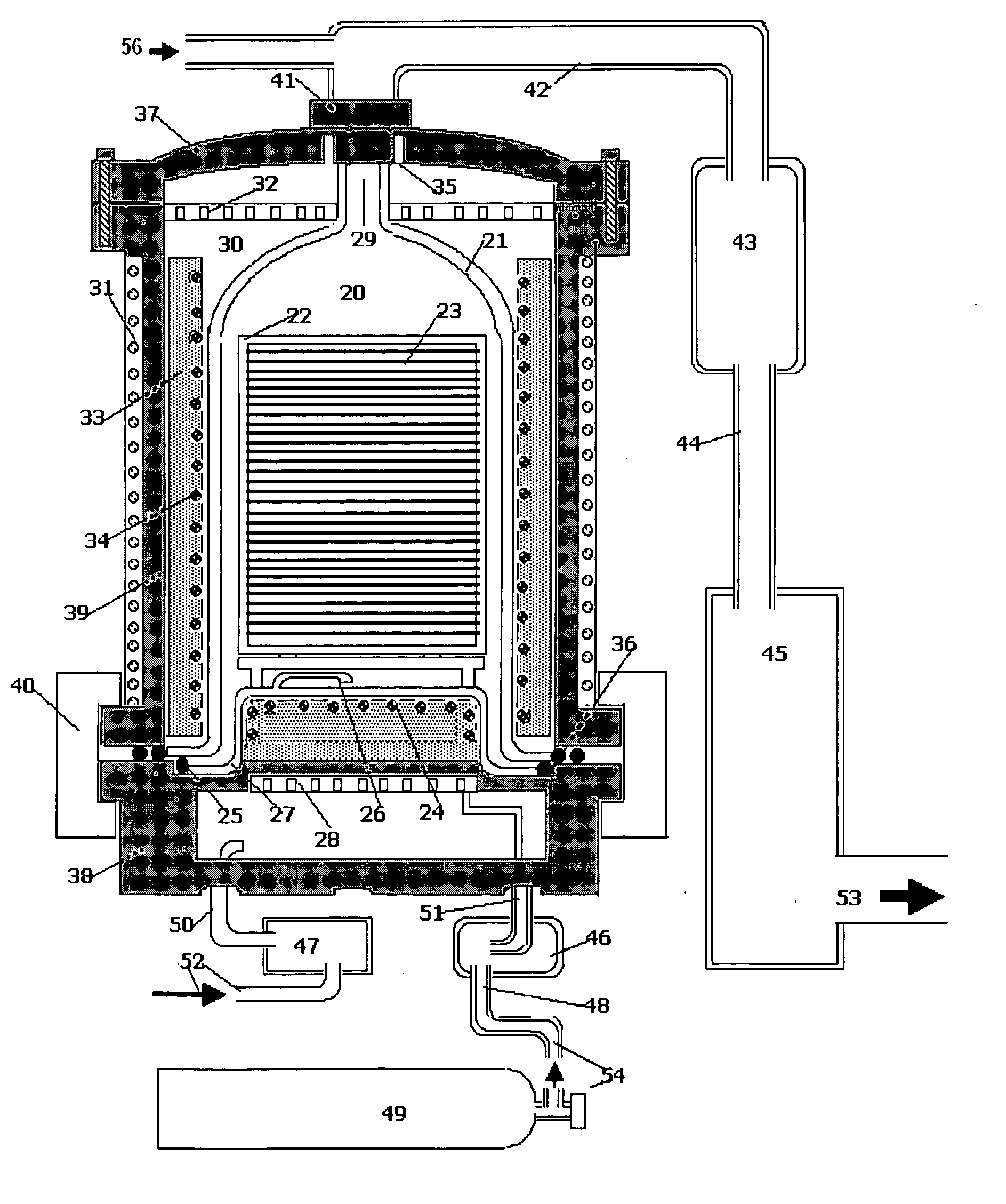
[0043] The present invention will now be described more fully hereinafter with reference to the accompanying drawings, in which various exemplary embodiments of the invention are shown. This invention may, however, be embodied in many different forms and should not be construed as limited to the embodiments set forth herein; rather, these embodiments are provided so that this disclosure will be thorough and complete, and will fully convey the scope of the invention to those skilled in the art. Likewise, for purposes of explanation, numerous specific details are set forth in the following description in order to provide a thorough understanding of the present invention. It will be evident, however, to one skilled in the art that the present invention may be practiced without these specific details.

[0044] One of the fundamental requirements in designing high pressure processing vessels using hydrogen or other hazardous gas is to ensure the safety. Under a controlled environment, the ...


PUM


Abstract

Novel methods and apparatuses for annealing semiconductor devices in a high pressure gas environment. According to an embodiment, the annealing vessel has a dual chamber structure, and potentially toxic, flammable, or otherwise reactive gas is confined in an inner chamber which is protected by pressures of inert gas contained in the outer chamber. The incoming gas delivery system and exhaust gas venting system are likewise protected by various methods. Embodiments of the present invention can be used, for example, for high-K gate dielectric anneal, post metallization sintering anneal, and forming gas anneal in the semiconductor manufacturing process.

Description

BACKGROUND OF THE INVENTION [0001] 1. Field of the Invention [0002] The present invention generally relates to semiconductor manufacturing process. More particularly, the present invention pertains to methods and apparatuses for high pressure gas annealing. [0003] 2. Description of the Related Art [0004] During the semiconductor manufacturing process, various different thermal treatments are performed on a semiconductor wafer, for example, during or following oxidation, nitridation, silicidation, ion implants, and chemical vapor deposition processes, to achieve effective reaction with the interface as well as the bulk of the semiconductor wafer. A hydrogen or deuterium passivation process is also a known practice performed at elevated temperature, typically at around 400° C.˜500° C. [0005] Key determining factors for effective reaction not only include the process temperature, but also the processing time and the concentration of a particular gas or a mixture of gases used for a par...

Claims


Application Information

Patent Timeline
IPC IPC(8): H01L21/00F27D11/00
CPCH01L21/324H01L22/12H01L2924/0002H01L2924/00
Inventor KIM, SANG-SHINRIVERA, MANUEL SCOTTHONG, SUK-DONG
Owner PSMC
Why Eureka
Try Eureka