Method for processing copper surface, method for forming copper pattern wiring and semiconductor device manufactured using such method

a technology of copper pattern wiring and processing method, which is applied in the direction of solid-state diffusion coating, coating, chemical apparatus and processes, etc., can solve the problems of metal nanoparticles, copper surface is oxidized, and it is difficult to deny the possibility of plasma damage, so as to achieve easy thermal decomposition and removal, clean copper surface, and easy removal

Inactive Publication Date: 2007-08-16
INVENSAS CORP
View PDF4 Cites 25 Cited by
  • Summary
  • Abstract
  • Description
  • Claims
  • Application Information

AI Technical Summary

Benefits of technology

[0019] According to the present invention, by causing a chemical species generated by a catalytic decomposition reaction of a compound containing hydrogen and nitrogen to react with a copper surface, a contaminant on the copper surface can be reduced and removed and a copper nitride protective film capable of readily removed can be formed on the copper surface. After that, by heating the copper surface on which the protective film is formed, the protective film is readily thermally decomposed and removed and a clean copper surface can be obtained and, therefore, a copper surface treatment method not requiring re-cleaning is provided. Also, according to the present invention, it is possible to form a protective film on the copper surface without changing the properties of a material other than copper on a substrate, for example, the permittivity of a dielectric material.
[0020] Also, according to the present invention, reduction is performed under a reduced pressure by use of atomic hydrogen (H) decomposed by a metal catalyst of the hot-wi

Problems solved by technology

However, in a case where a process is interrupted in the course of the process and a copper surface has to be exposed to the air for a long time or in a case where a copper surface has to be exposed to an oxidizing atmosphere in the course of the process, it has often been necessary to perform the re-cleaning of the copper surface in the course of the process.
However, the case of the techniques using plasma poses the problem that it is impossible to deny the possibility that what is called plasma damage occurs.
However, the copper surface is oxidized also during this heat treatment.
In metal nanoparticles, the proportion of atoms in the surface portion is large and, therefore, metal nanoparticles have the problem that interconnect resistance increases due to the formation of surface copper oxides.
Because an organic solvent cann

Method used


Image

  • Method for processing copper surface, method for forming copper pattern wiring and semiconductor device manufactured using such method
  • Method for processing copper surface, method for forming copper pattern wiring and semiconductor device manufactured using such method
  • Method for processing copper surface, method for forming copper pattern wiring and semiconductor device manufactured using such method

Examples


embodiment 1

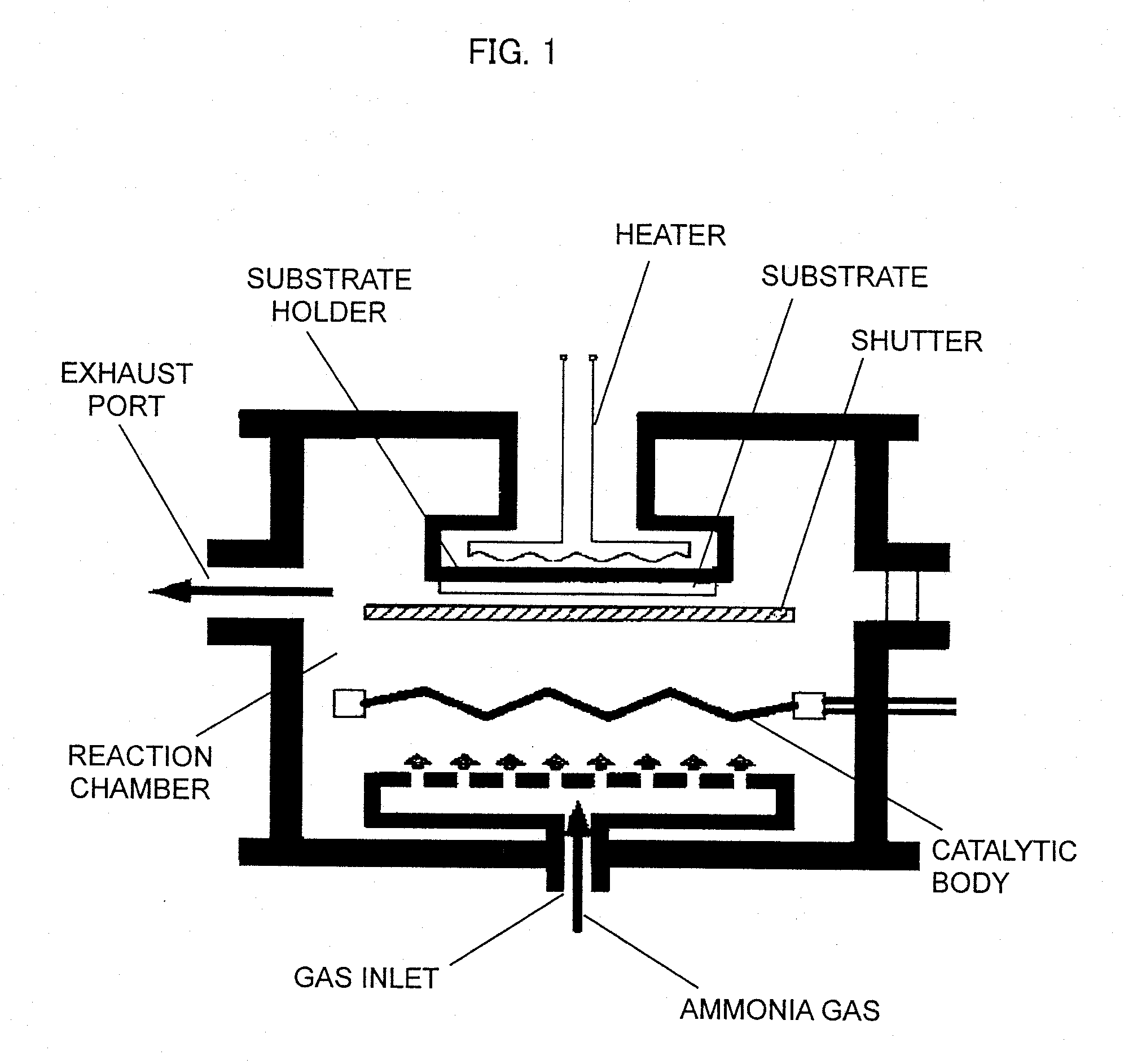
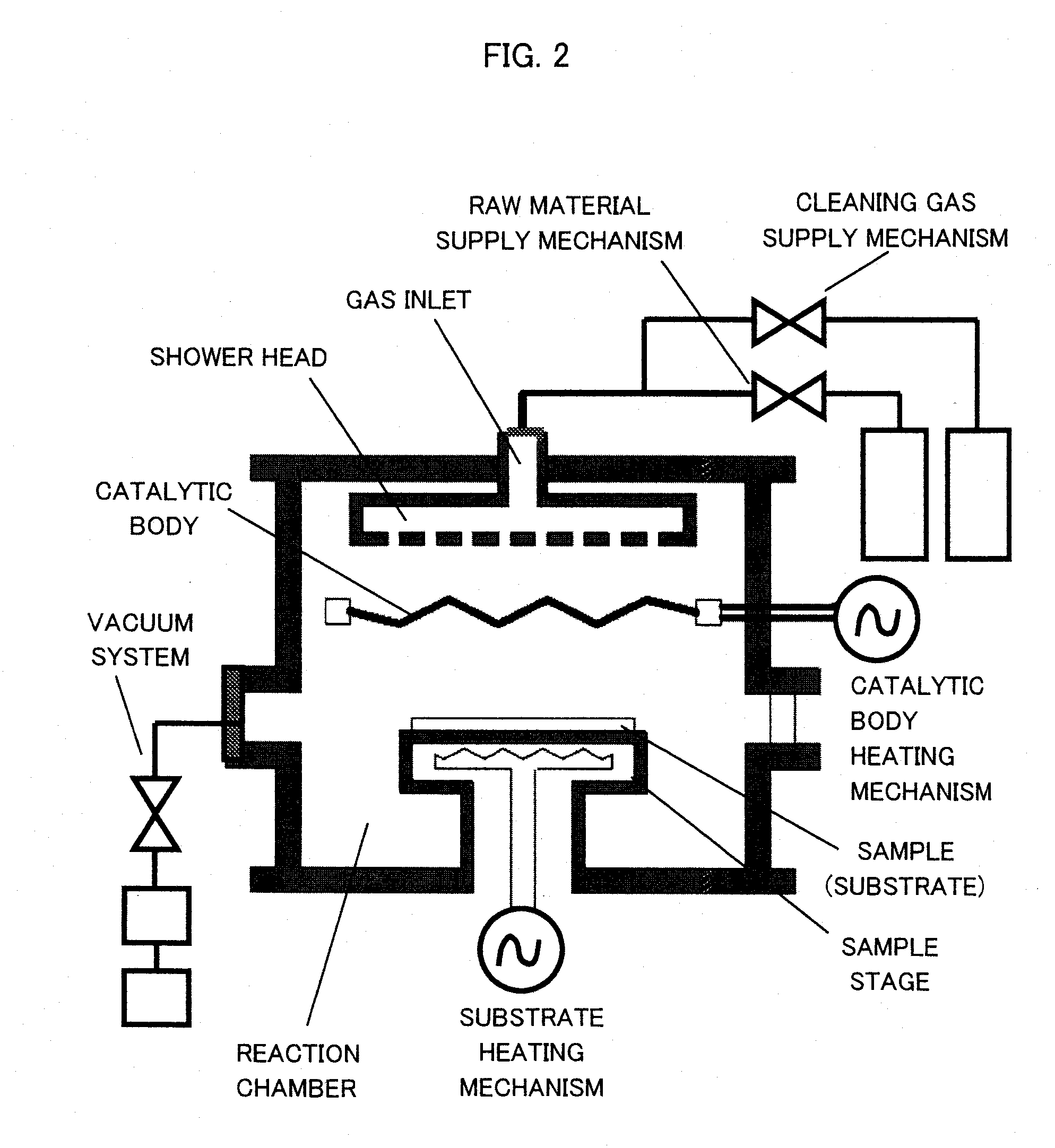
[0048] By use of the reactor shown in FIG. 1, a silicon LSI wafer in which copper interconnects had been formed by the damascene process was placed as a substrate on the substrate holder. The temperature of the substrate holder was heated to 60° C., the catalytic body of a tungsten wire was heated to 1600° C., and the pressure in the reaction chamber was set at 2.7×10⁻⁵ Pa. First, contamination was removed from the silicon LSI wafer in which copper interconnects had been formed by the damascene process and in order to continuously form a protective film of a copper surface, ammonia gas was caused to flow at a flow rate of 50 sccm for 20 minutes, whereby the ammonia gas treatment of the silicon substrate was performed. By this treatment, the removal of the contamination and the formation of a protective film on the copper surface from which the contamination had been removed were performed in order.

[0049]FIG. 3 shows spectra obtained by the X-ray photoelectron spectroscopy (XPS) whe...

embodiment 2

[0052] The above-described silicon LSI substrate on which a copper protective film had been deposited after being allowed to stand was again put into the above-described reaction chamber and subjected to a heat treatment in a vacuum. From the measurement results of the X-ray photoelectron spectroscopy (XPS), it became apparent that when the treatment is performed at 350° C. for 150 minutes, the copper protective film is completely thermally decomposed and removed.

embodiment 3

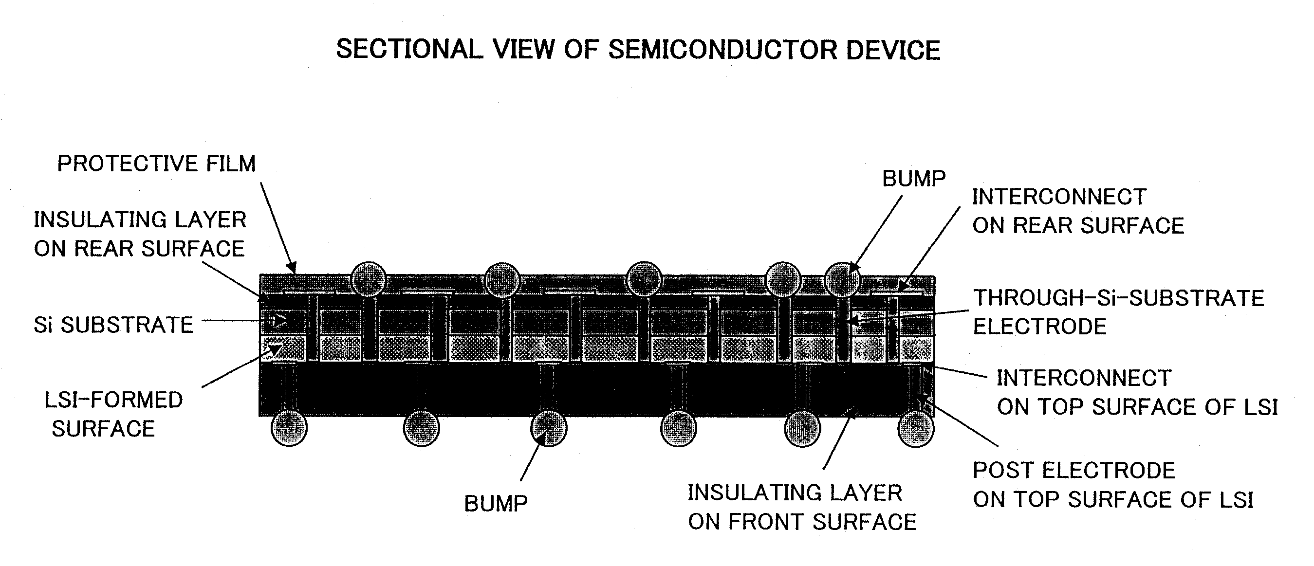
[0053]FIG. 6 is a diagram which shows an example in which the technique of the present invention for removing contamination due to an organic solvent and oxides is applied to a semiconductor device. In the illustrated semiconductor device, an LSI-formed surface is present on the top surface of an Si substrate. A circuit (a circuit element) is formed on the LSI-formed surface. In the figure, the side where this LSI-formed surface is present is called the top surface side, and the reverse side is called the rear surface side. And the semiconductor device is illustrated, with this top surface side facing downward.

[0054] The semiconductor substrate (Si substrate) having the LSI-formed surface is provided with a through-Si-substrate electrode which connects the top surface side and the rear surface side. On this top surface side (the bottom side in the figure), a multilayer interconnect portion (a interconnect on the top surface of the LSI) is formed on the LSI-formed surface. Furthermo...


PUM


Abstract

A gas inlet is disposed in a lower portion of a reaction chamber, a copper substrate is disposed in an upper portion thereof, and a tungsten catalytic body heated to 1600° C. is disposed midway between the two. Ammonia gas introduced from the gas inlet is decomposed by the tungsten catalytic body, a chemical species generated by the decomposition reacts with a surface of the copper substrate, and reduces and removes a contaminant on the copper surface, and a Cu3N thin film is formed on the copper substrate surface. This Cu3N film has the action of a film which prevents the oxidation of copper. This Cu3N film is thermally decomposed and removed when heated to temperatures of not less than 300° C., leaving a clean copper surface behind.

Description

TECHNICAL FIELD [0001] The present invention relates to a method of processing a copper surface which involves reducing and removing a contaminant on the copper surface, simultaneously forming a copper surface protective film capable of being easily removed, and removing the protective film from the copper surface on which the protective film is formed, a copper metal nanoparticle formed by this treatment method, a method of forming a patterned copper interconnect in which a decrease in resistance after interconnect formation is aimed at in forming a patterned interconnect by a direct writing technique using copper metal nanoparticles, and a semiconductor device fabricated by using this method. BACKGROUND ART [0002] A copper surface is apt to be readily oxidized. When during a process a copper surface is allowed to stand in the air for a long time or comes into contact with an oxidizing atmosphere, the copper surface is oxidized and it is necessary to perform an intermediate treatme...

Claims


Application Information

Patent Timeline
IPC IPC(8): H01L23/12H01L21/00B08B7/00C01B21/06C23C8/02C23C8/24C23C8/80C23F15/00C23G5/00H01L21/02H01L21/3205H01L21/321H01L21/768
CPCB08B7/00C23C8/02C23C8/24H01L21/76838C23G5/00H01L21/02068H01L21/321C23C8/80H01L2224/11H01L2224/14181Y10S977/773Y10S977/777
Inventor IZUMI, AKIRA
Owner INVENSAS CORP
Why Eureka
Try Eureka