Monolithic high aspect ratio nano-size scanning probe microscope (SPM) tip formed by nanowire growth

a scanning probe and nanowire technology, applied in the field of scanning microscope probes, can solve the problems similar to micro-machined afm tips, and achieve the effects of low cost of manufactured tips, easy growth, and reliability and durability advantages

Inactive Publication Date: 2007-09-27
GLOBALFOUNDRIES INC
View PDF6 Cites 40 Cited by
  • Summary
  • Abstract
  • Description
  • Claims
  • Application Information

AI Technical Summary

Benefits of technology

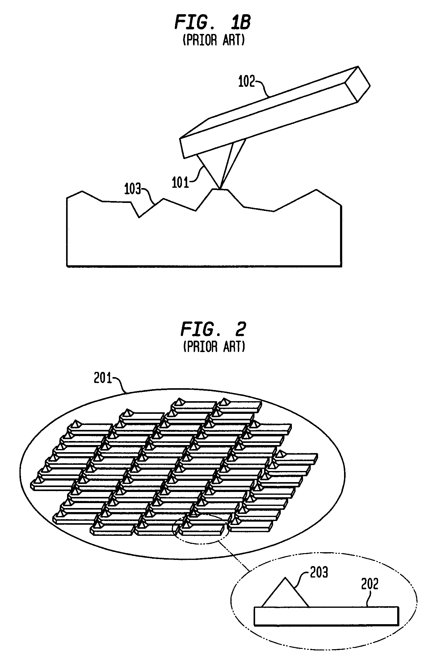
[0009] The inventive structure and methods described herein provide several advantages over the prior art. First, the fabrication of the tips is a batch process in which all steps are conventional silicon processing steps. As such, many tips can be fabricated in parallel on a single silicon wafer as illustrated by FIG. 2. As a result, the cost of the manufactured tip is expected to be low and similar to that of a micromachined AFM tip. Moreover, the performance delivered by the tip disclosed in the present invention is that of a high aspect ratio nanometer size radius tip that currently cost 1000× more than

Problems solved by technology

As a result, the cost of the manufactured tip is expected

Method used


Image

  • Monolithic high aspect ratio nano-size scanning probe microscope (SPM) tip formed by nanowire growth
  • Monolithic high aspect ratio nano-size scanning probe microscope (SPM) tip formed by nanowire growth
  • Monolithic high aspect ratio nano-size scanning probe microscope (SPM) tip formed by nanowire growth

Examples


example

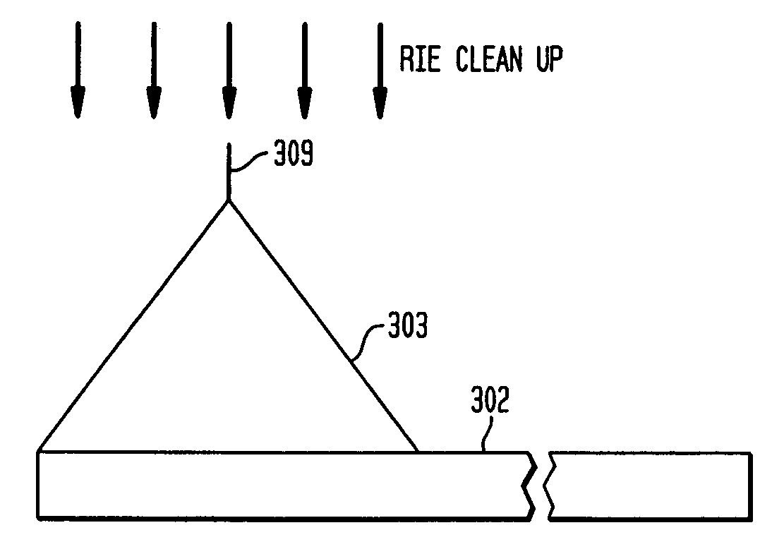
[0047] In this example, a micromachined silicon pyramid extended by a silicon nanowire using the method outlined in FIGS. 3A-3C was provided. Specifically, a silicon wafer was masked and etched in KOH to form silicon pyramids. The native oxide was removed by an HF dip and a 2 nm thick gold film was evaporated over the silicon pyramid. The wafer was then loaded into an UHV-CVD furnace. A pre-growth anneal at 500° C. in H2 ambient for 10 minutes was used to agglomerate the Au film into AuSi eutectic droplets. The furnace temperature was then lowered to the nanowire growth temperature of 420° C. Pure silane (SiH4) at a pressure of 2 torr was used as the precursor. FIGS. 6A-6B are SEM images showing a silicon pyramid following the growth. The typical length of the silicon nanowires is about 700 nm and their typical diameter is about 10-12 nm.

[0048] Following the growth the wafer was etched by RIE using CF4 chemistry. As can be seen in FIGS. 7A-7B the non-vertical nanowires are etched o...


PUM

PropertyMeasurementUnit
Diameteraaaaaaaaaa
Lengthaaaaaaaaaa
Electrical conductoraaaaaaaaaa

Abstract

A scanning probe where the micromachined pyramid tip is extended by the growth of an epitaxial nanowire from the top portion of the tip is disclosed. A metallic particle, such as gold, may terminate the nanowire to realize an apertureless near-field optical microscope probe.

Description

FIELD OF THE INVENTION [0001] The present invention relates to scanning microscope probes, and more specifically to a monolithic silicon probe made of an etched silicon pyramid with its tip extended with a Si nanowire. The present invention also relates to methods of fabricating the silicon probe and the nanowire extension. BACKGROUND OF THE INVENTION [0002] Scanning Probe Microscopy (SPM) techniques such as Atomic Force Microscopy (AFM) and Near-Field Scanning Optical Microscopy (NSOM) are very useful techniques for the study of surfaces. Acquired SPM images provide surface properties (e.g., topography or roughness) on a nanometer scale. As a result, SPM instruments are now used routinely for testing in industries where small dimensions are involved. A typical example is the semiconductor industry where AFM is used to evaluate the surface roughness and topography following a film deposition or a chemical mechanical polishing (CMP) step. Another important application of AFM in the s...

Claims


Application Information

Patent Timeline
IPC IPC(8): G01N23/00G01Q70/12B81C99/00G01Q60/22G01Q60/38G01Q70/16
CPCB82Y15/00B82Y20/00G01Q70/12G01Q60/22B82Y35/00
Inventor COHEN, GUY M.HAMANN, HENDRIK F.
Owner GLOBALFOUNDRIES INC
Why Eureka
Try Eureka