Charge Neutralizing Device

a charge neutralizing device and charge technology, applied in plasma technique, nuclear engineering, therapy, etc., can solve the problems of poor coupling efficiency between the supplied electronic current and the beam plasma, the device is charged to split or diverge the beam, and it is difficult to perform high current ion implantation using the known charge neutralizing device, etc., to achieve high density plasma, low energy, and high reliability

Inactive Publication Date: 2007-10-04
PANASONIC CORP
View PDF17 Cites 9 Cited by
  • Summary
  • Abstract
  • Description
  • Claims
  • Application Information

AI Technical Summary

Benefits of technology

[0041] As described above, it is possible to generate high density plasma having low energy in the invention.
[0042] Additionally, a semiconductor device that is produced using a charge neutralizing device, an ion implanting device, and a beam line device according to the invention and has an internal voltage of 1 V or less can have high reliability.
[0043] Furthermore, an object, such as an electron device, which is produced by using the charge neutralizing device, the ion implanting device, and the beam line device according to the invention is advantageous in that charge neutralization is efficiently performed and reliability is high. Accordingly, in the case of when long life or high reliability is needed, such as rockets for space development, the device can be used.

Problems solved by technology

However, in the above-mentioned technology, even though charge neutralization occurs at a point close to the electron source, the charge neutralization may not occur at the opposite point (the point that is furthest from the electron source), causing charges of the device to split or divergence of the beam.
Additionally, in a beam-scanning type an ion implanter, the coupling efficiency of supplied electronic current and beam plasma is poor, thus it is very difficult to perform high current ion implantation using the known charge neutralizing device.
Accordingly, there is a problem in that high-speed electrons having energy of 300 eV charge the substrate 13 such that the substrate has a negative charge.
Furthermore, cracking occurs due to the negative charge, and the gate insulating film 22 deteriorates even if the cracking does not occur.

Method used


Image

  • Charge Neutralizing Device
  • Charge Neutralizing Device
  • Charge Neutralizing Device

Examples


first embodiment

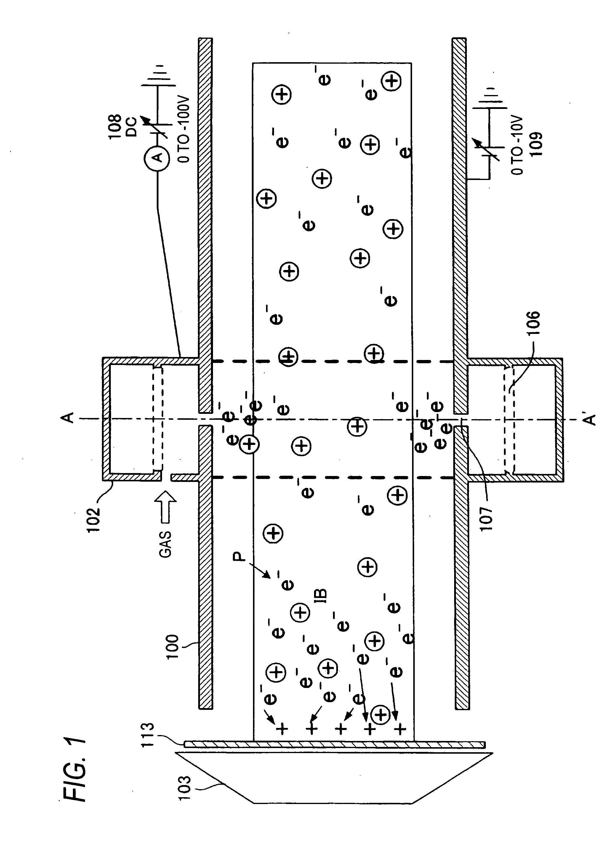
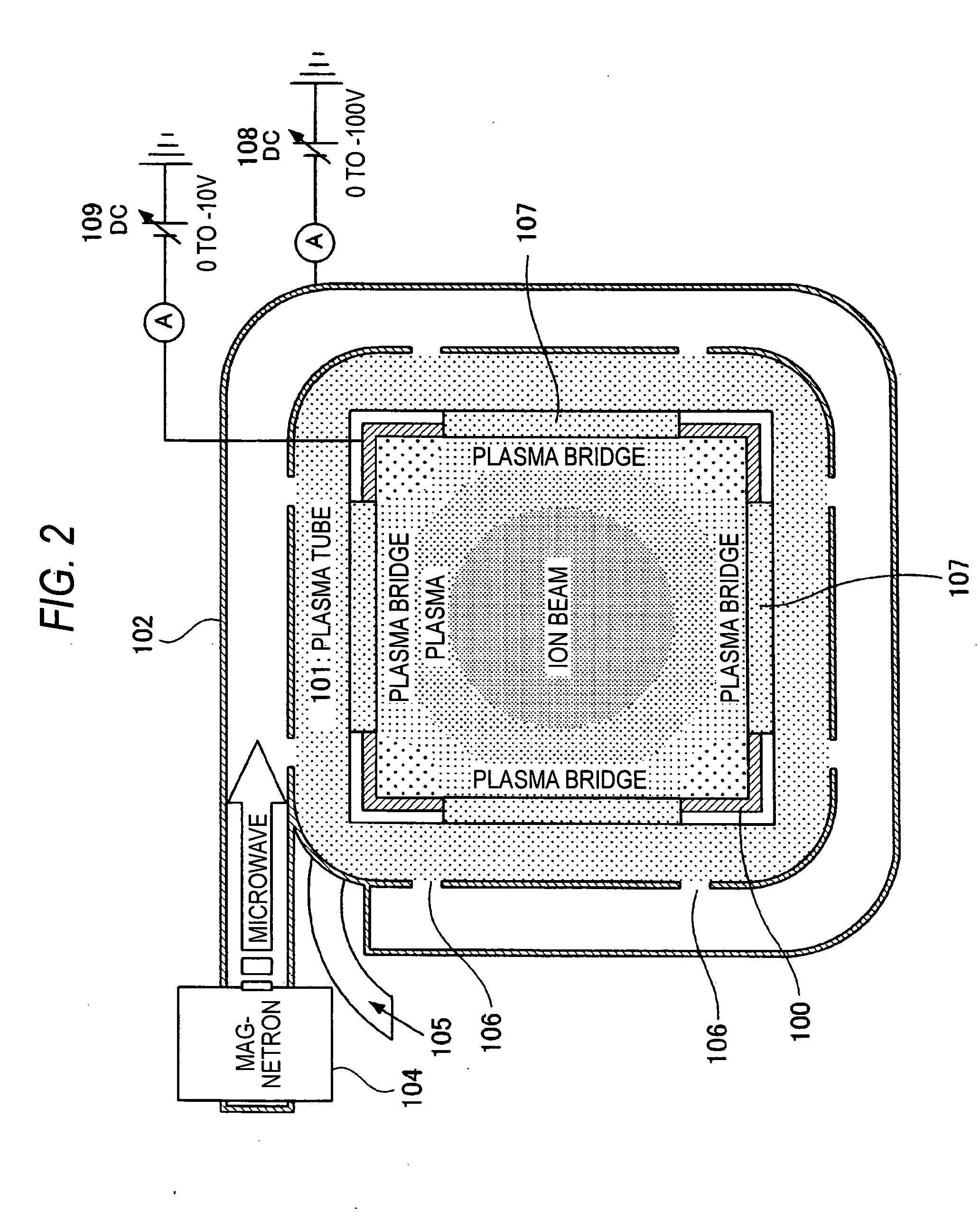
[0101] As shown in a cross-sectional view of FIG. 1 and a cross-sectional view of FIG. 2 that is taken along the line A-A′ of FIG. 1, a charge neutralizing device of this embodiment radiates a beam plasma P that includes an ion beam IB supplied from a plasma generator (not shown) onto a silicon wafer 113 that is a substrate to be treated on a wafer support 103, and prevents charge of the silicon wafer.

[0102] The charge neutralizing device is provided with a plasma tube 101 and a waveguide 102. The plasma tube 101 is disposed at a predetermined position of a conductive tube 100 that is a path through which the ion beam IB passes so as to surround a circumference of a side of the conductive tube perpendicular to the axis of the conductive tube. The waveguide 102 is disposed so as to surround an external surface of the plasma tube 101. Electron plasma is generated in the plasma tube 101 to compensate for lack of electrons of the beam plasma P surrounding the ion beam IB, thereby preve...

second embodiment

[0127] In the above-mentioned first embodiment, the plasma tube 101 and the waveguide 102 are provided. The plasma tube 101 is disposed so as to surround the circumference of the side of the conductive tube perpendicular to the axis of the conductive tube. The waveguide 102 is disposed so as to surround the external surface of the plasma tube 101, and electron plasma is generated in the plasma tube 101. A charge neutralizing device according to this embodiment is shown in the cross-sectional view of FIG. 3 and the cross-sectional views of FIGS. 4 and 5 that are taken along the lines A-A and B-B of FIG. 3. This embodiment is different from the first embodiment in that the plasma tube 101 and the waveguide 102 are adjacent to each other to surround the conductive tube 100. In this embodiment, plasma excitement is performed using a progressive wave.

[0128] Additionally, the electric potential for controlling bias is supplied from a second power source 108 through a bias wire 110 dispos...

third embodiment

[0133] In the second embodiment, plasma excitement using a progressive wave is described. However, the excitement may be performed using a stationary wave.

[0134] The third embodiment is the same as the second embodiment, except that the waveguide 102 has a closed pipe structure to form the stationary wave as shown in the cross-sectional view of FIG. 6 taken in the direction perpendicular to the beam.

[0135] The cross-sectional view that is taken in the direction parallel to the beam is the same as that of FIG. 3.

[0136] In this embodiment, the plasma tube 101 and the waveguide 102 are adjacent to each other to surround the conductive tube 100, and plasma excitement is performed using the stationary wave.


PUM


Abstract

Disclosed is a charge neutralizing device which is capable of being applied to a substrate 13 having a large area and in which electrons having low energy of 5 eV or less, and preferably 2 eV, are supplied so that charge due to ion implantation and damage by the electrons are avoided with respect to a cusp device. The charge neutralizing device includes a microwave generating unit, a plasma generating unit that generates electron plasma using a microwave generated from the microwave generating unit, and a contact unit that brings the electron plasma generated from the plasma generating unit into contact with a beam plasma region including an ion beam.

Description

RELATED APPLICATIONS [0001] This application is the U.S. National Phase under 35 U.S.C. § 371 of International Application No. PCT / JP2005 / 009460, filed on May 24, 2005, which in turn claims the benefit of Japanese Application No. 2004-183112, filed on May 25, 2004, the disclosures of which Applications are incorporated by reference herein.TECHNICAL FIELD [0002] The present invention relates to a charge neutralizing device and, more particularly, to a charge neutralizing device that is applied to an ion implanting device used to form an impurity layer on a semiconductor substrate during a process of producing a semiconductor, a semiconductor device produced using the same, and an electronic element, such as a liquid crystal panel, on which the semiconductor device is mounted. BACKGROUND ART [0003] In a known technology for producing semiconductors, a process of ion implanting various types of conductive impurities, such as boron (B), phosphorus (P), and arsenic (As), as a solid gas o...

Claims


Application Information

Patent Timeline
Patent Type & Authority Applications(United States)
IPC IPC(8): G21K5/00H01J7/24G21K1/14H01J37/20H01J37/317H01L21/265H05H1/24H05H1/46
CPCG21K1/14H01J37/026H05H1/46H01J2237/0044H01L21/26513H01J37/3171H01J37/30H01L21/265
Inventor ITO, HIROYUKISAKUDO, NORIYUKISASAKI, YUICHIROMIZUNO, BUNJI
Owner PANASONIC CORP
Why Eureka
Try Eureka