Field effect transistor, organic thin-film transistor and manufacturing method of organic transistor

Inactive Publication Date: 2008-01-17
HITACHI LTD
View PDF9 Cites 16 Cited by
  • Summary
  • Abstract
  • Description
  • Claims
  • Application Information

AI Technical Summary

Problems solved by technology

At present, it is difficult to give plasticity to a TFT using amorphous silicon and polycrystalline silicon, and since vacuum apparatus is used for the manufacturing process thereof, the manufacturing cost is high in general.
However, for the manufacture of an organic TFT formed of low molecule whose performance can be improved easily, the vacuum deposition is used in general, and it is disadvantageous in terms of a manufacturing aspect.
Meanwhile, an organic TFT formed of high molecule which is advantageous in terms of manufacturing cost is particularly low in performance as TFT and it can be applied only to the limited uses.
Although some causes t

Method used


Image

  • Field effect transistor, organic thin-film transistor and manufacturing method of organic transistor
  • Field effect transistor, organic thin-film transistor and manufacturing method of organic transistor
  • Field effect transistor, organic thin-film transistor and manufacturing method of organic transistor

Examples


first embodiment

[0029]In this embodiment, the discussion of the Non-Patent Document 8 is extended, and a method for obtaining the Schottky barrier Φ at the electrode / organic semiconductor interface from physical constants of the constituent elements of the electrode and semiconductor is provided. As the combinations of an electrode and organic semiconductor, there are hydrogen-terminated silicon surface / polythiophene polymer, gold / pentacene crystal, gold / various thiol monomolecular film, silver / various thiol monomolecular film, and others, and electron states thereof are examined by the logical computation by first principle calculation and the electron state measurement using a scanning tunnel microscope. As a result, it can be found that the Schottky barrier Φ can be estimated using the following formulas 7 to 11.

[0030]More specifically, when the carriers are electrons, the Schottky barrier Φ can be obtained by the formula 7.

Φ=γB(φM−χS)+(1+γB)Eg / 2   (formula 7)

[0031]Here, the following formulas 8...

second embodiment

[0035]In this embodiment, an example of CTFT according to the present invention will be disclosed.

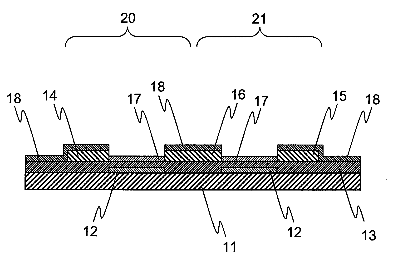
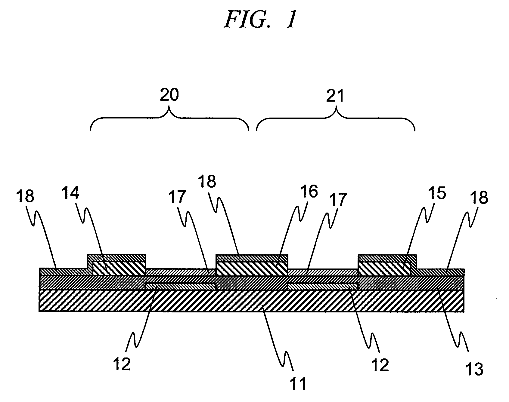
[0036]FIG. 1 is a cross-sectional view schematically showing a structure of a CTFT according to the present invention. In FIG. 1, an organic semiconductor thin film 17 is a polycrystalline pentacene thin film made of pentacene crystal grains in this embodiment. The CTFT is composed of a source electrode 14 and a source electrode 15, an organic semiconductor thin film 17, a common drain electrode 16, and two gate electrodes 12. The CTFT has a structure where an n channel FET 20 and a p channel FET 21 are connected in series. In this embodiment, the source electrode 15 functions as a ground electrode and the source electrode 14 functions as an operation voltage applying electrode, and common voltage signals are inputted to the two gate electrodes 12 and the drain electrode 16 functions as an output electrode. A liquid repellent region 18 is a region with high liquid repellency, and by mak...

third embodiment

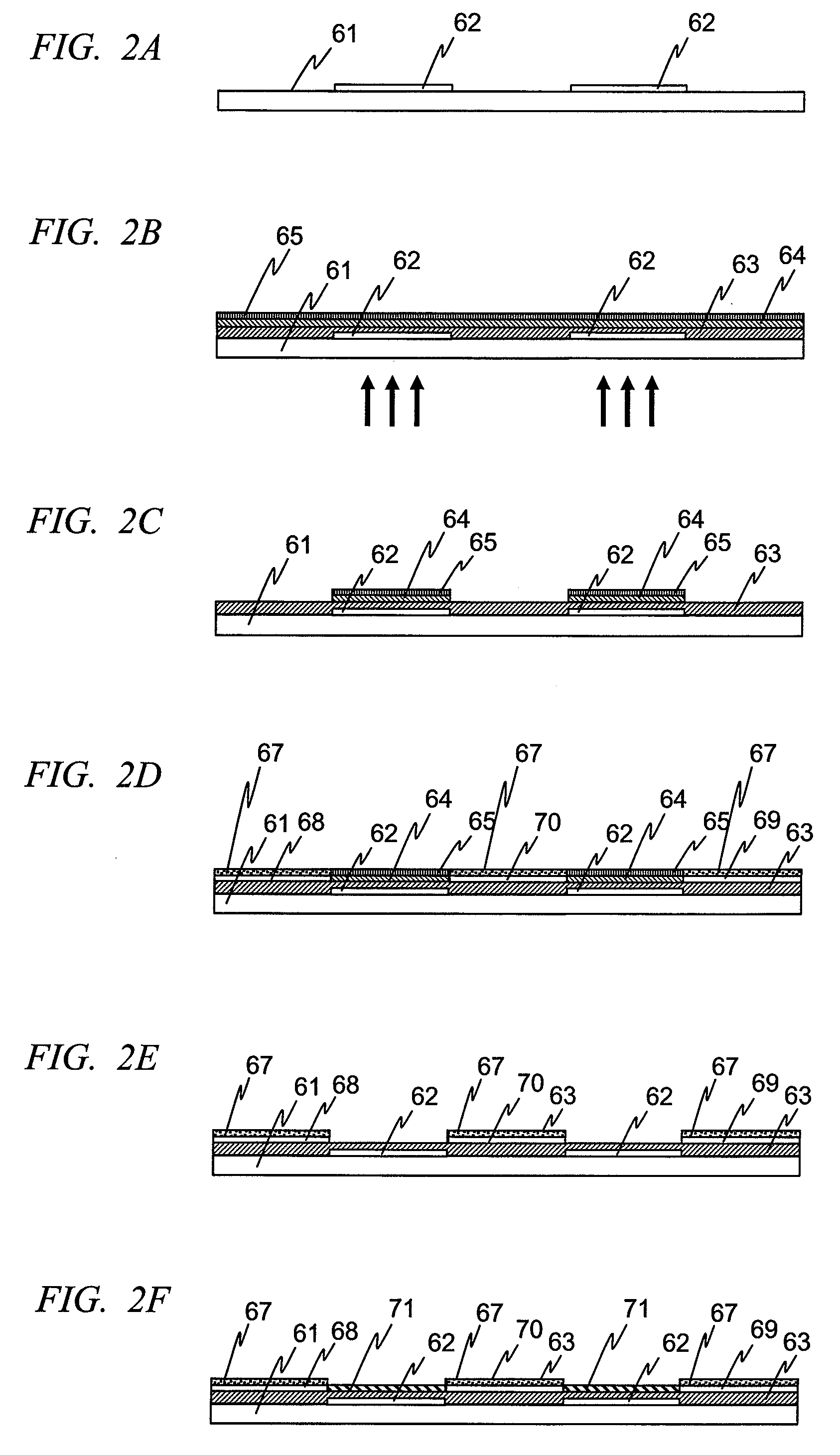
[0039]In this embodiment, an example of a manufacturing method of a CTFT formed by the present invention will be disclosed. FIG. 2A to FIG. 2F are sectional views showing an example of a manufacturing method of a CTFT formed by the present invention. In this embodiment, a manufacturing method of an organic thin-film CTFT according to the present invention will be described, in which a material with plasticity is used and printing process and coating process are employed instead of lithography. FIG. 2A to 2F are cross-sectional views for describing the manufacturing method specifically.

[0040]As shown in FIG. 2A, gate electrodes 62 are printed using conductive ink on a plastic substrate 61. Since the gate electrodes 62 are formed by baking the printed ink, it is necessary to pay attention to the softening temperature of the substrate 61 because a plastic substrate is used for the substrate 61. In this embodiment, since a high heat-resistant transparent polyimide sheet with a thickness...


PUM


Abstract

A method for determining the combination of the electrode and organic semiconductor with improved electron injection efficiency and hole injection efficiency in an organic TFT is provided, two types of FETS, that is, an n channel FET and a p channel FET are realized, and further, a complementary TFT (CTFT) is provided. The method for obtaining the vacuum level shift at the electrode metal/organic semiconductor interface from physical constants of constituent elements of the electrode and the organic semiconductor is provided. By changing the electrode metal through an electrochemical method, the electrodes whose electron injection and hole injection can be controlled are formed. By using these electrodes, two types of FETs such as an n channel FET and a p channel FET are realized, thereby providing a complementary TFT (CTFT).

Description

CROSS-REFERENCE TO RELATED APPLICATION[0001]The present application claims priority from Japanese Patent Application No. JP 2006-192292 filed on Jul. 13, 2006, the content of which is hereby incorporated by reference into this application.TECHNICAL FIELD OF THE INVENTION[0002]The present invention relates to a field effect transistor (FET), an organic thin-film transistor, and a manufacturing method of an organic transistor. More particularly, it relates to a thin-film transistor (TFT) using organic semiconductor for its channel. Furthermore, it relates to a so-called CTFT (Complementary TFT) in which two types of FETs, that is, a FET whose carriers passing through its channel are electrons (n channel TFT) and a FET whose carriers are holes (p channel TFT) are connected in series and a manufacturing method thereof.BACKGROUND OF THE INVENTION[0003]In a thin-type display device using an organic EL (Electro Luminescence) element and liquid crystal, a thin-film transistor (TFT) using am...

Claims


Application Information

Patent Timeline
IPC IPC(8): H01L51/10H01L51/40
CPCH01L51/0021H01L51/105H01L51/0545H10K71/60H10K10/466H10K10/84H10K10/481H10K10/82
Inventor HASHIZUME, TOMIHIROFUJIMORI, MASAAKISUWA, YUJIARAI, TADASHI
Owner HITACHI LTD
Why Eureka
Try Eureka