Multilayered printed circuit board, solder resist composition, multilayered printed circuit board manufacturing method, and semiconductor device

a printed circuit board and multi-layer technology, applied in printed circuit manufacture, non-metallic protective coating applications, metallic pattern materials, etc., can solve the problems of cracking and peeling, affecting the performance of the printed circuit board, and generating stress on the solder resist layer

Inactive Publication Date: 2008-02-21
IBIDEN CO LTD
View PDF23 Cites 43 Cited by
  • Summary
  • Abstract
  • Description
  • Claims
  • Application Information

AI Technical Summary

Benefits of technology

[0024] The present invention is developed to solve the above described problems and an objective of the present invention is to provide a multilayered printed circuit board free from cracks attributed to thermal expansion difference between a solder resist layer and another part during the manufacturing process of the multilayered printed circuit board or after an IC chip is mounted on the multilayered printed circuit board, to provide a solder resist composition to be used for the manufacture of the multilayered printed circuit board, and to provide a method for manufacturing a multilayered printed circuit board using said solder resist composition.

Problems solved by technology

Hence, considerable stress is generated to the solder resist layer and, in some cases, cracks take place in the solder resist layer, or the solder resist layer is peeled from the under-fill or the interlaminar resin insulating layer.
Such cracking and peeling even take place with the heat at the time of forming the solder bump.
Also, cracking occurs more easily in a heat cycle test and in a reliability test under a high temperature and a high humidity, in which the multilayered printed circuit board is tried in severe condition.
If cracks are once formed in the solder resist layer, the insulation between the conductor circuit under the solder resist layer and the solder bump cannot be retained, thus to result in a degradation of the high insulating property and the reliability.
Further, since a mixture of an epoxy resin, an acrylic resin and the like is used for the interlaminar resin insulating layer in a conventional multilayered printed circuit board manufactured by the above described method, the dielectric constant and the dielectric loss tangent are high in a GHz band and, in this case, if a LSI chip and the like using high frequency signals in the GHz band are mounted on this, signal delay and signal error sometimes occur attributed to the high dielectric constant of the interlaminar resin insulating layer.
Therefore, if the dielectric constant and the dielectric loss tangent of a solder resist layer are high, it sometimes occurs a problem that signal delay and the like: in the bumps for the outer terminals of the solder resist layer; and in the inter-circuits are caused attributed to electromagnetic inter-reaction among circuits and the high dielectric property of the insulating layers existing in the surrounding of the circuits.
Further, even in the case that a multilayered printed circuit board for which a polyphenylene ether resin with a low dielectric loss tangent and a low dielectric constant and which does not induce easily the signal delay and signal error just as described above is used for the interlaminar resin insulating layers, such an effect is offset if the dielectric constant of a solder resist layer is high, therefore, signal delay and signal error sometimes take place.
However, the multilayered printed circuit board comprising a solder resist layer formed by using a conventional solder resist composition has not been satisfactory in terms of flame retardancy.

Method used


Image

  • Multilayered printed circuit board, solder resist composition, multilayered printed circuit board manufacturing method, and semiconductor device
  • Multilayered printed circuit board, solder resist composition, multilayered printed circuit board manufacturing method, and semiconductor device
  • Multilayered printed circuit board, solder resist composition, multilayered printed circuit board manufacturing method, and semiconductor device

Examples


example 1

A. Preparation of a Resin Composition for Roughened-Surface Formation for an Upper Layer

[0363] (i) A mixture composition was produced by blending 35 parts by weight of a resin solution produced by dissolving a cresol novolak type epoxy resin acrylated in 25% (made by Nippon Kayaku Co., Ltd.: molecular weight 2,500) of 80 wt. % concentration in diethylene glycol dimethyl ether (DMDG), 3.15 parts by weight of a photosensitive monomer (made by Toagosei Chemical Industry Co., Ltd.: Aronix M 315), 0.5 parts by weight of a defoaming agent (made by San Nopco Ltd.: S-65), and 3.6 parts by weight of N-methylpyrrolidone (NMP) in a container and mixing and stirring them.

[0364] (ii) Another mixture composition was produced by blending 12 parts by weight of polyether sulfone (PES), 7.2 parts by weight of an epoxy resin particle (made by Sanyo Chemical Industries, Ltd.: Polymerpol) with the average particle size of 1.0 μm and 3.09 parts by weight of the particle with the average particle size o...

example 2

A. Preparation of a Resin Composition for Roughened-Surface Formation for an Upper Layer and an Under Layer and Preparation of the Resin Filler were Carried Out in the Same Manner as Described in the Example 1

B. Method for Manufacturing a Multilayered Printed Circuit Board

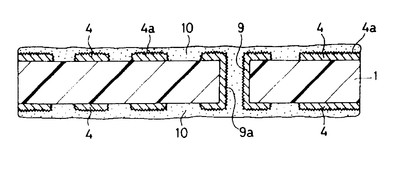
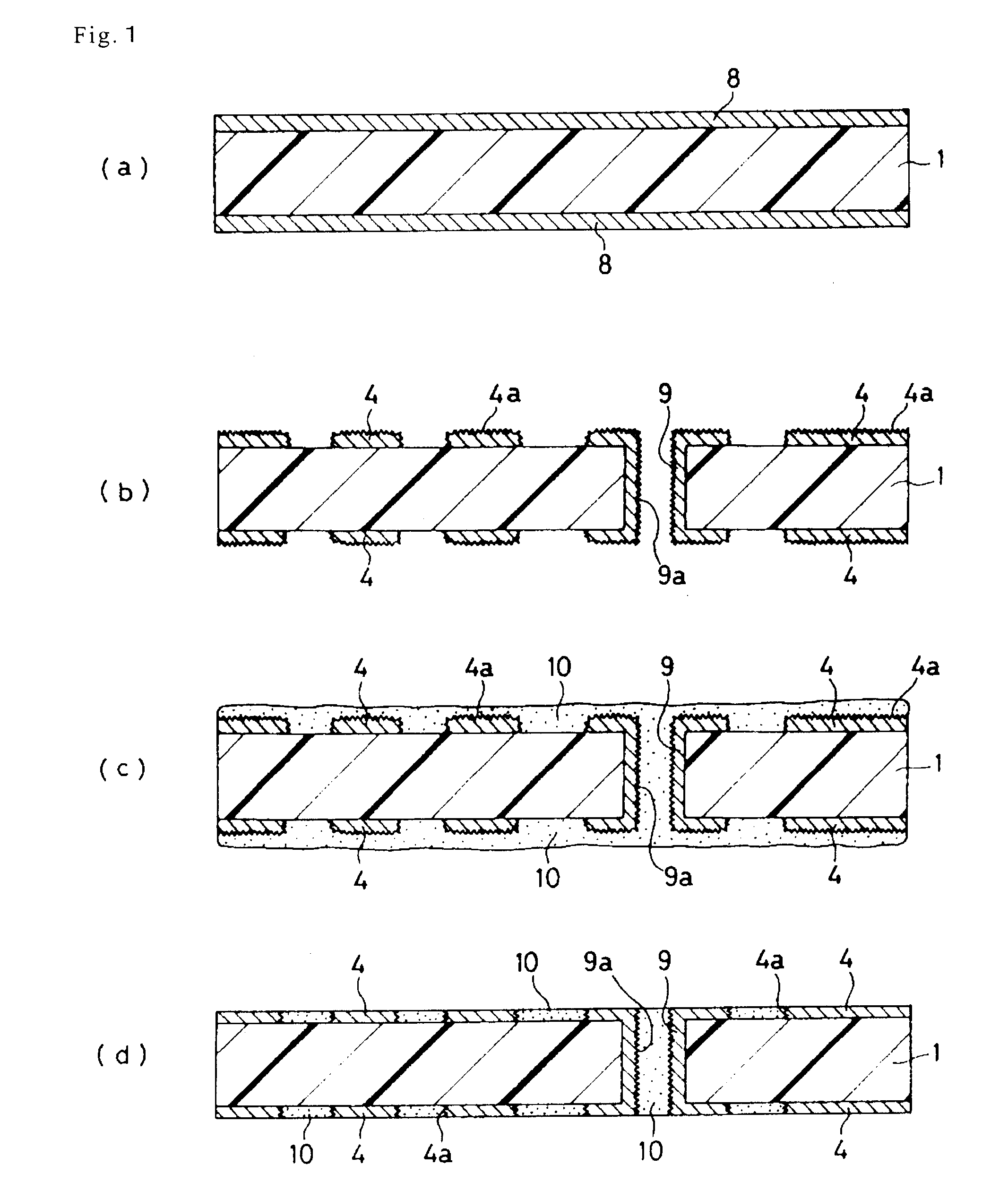
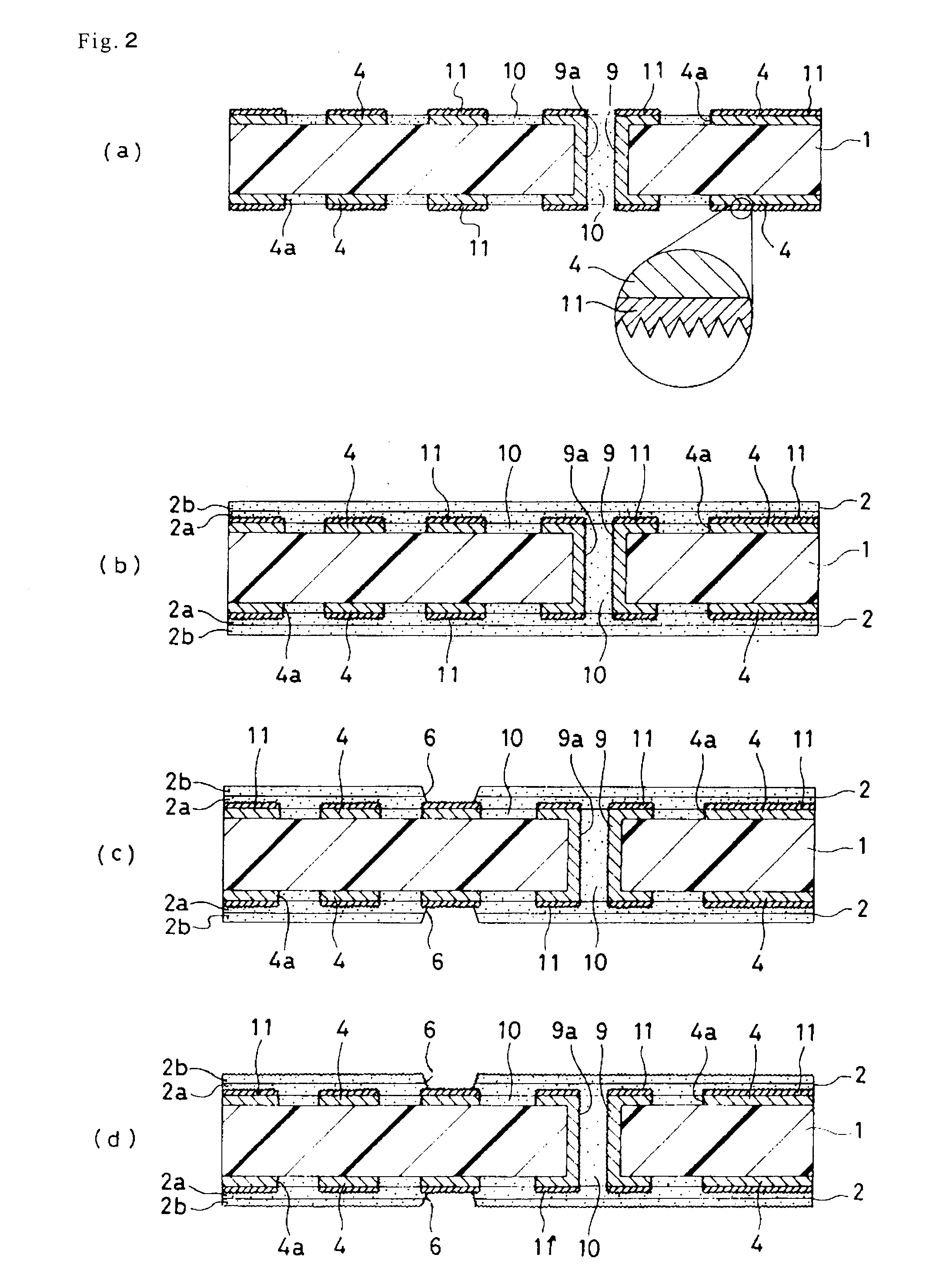
[0402] (1) A copper-laminated laminate plate composed of a substrate 1 which is made of a 1.0 mm-thick glass epoxy resin or BT (bismaleimide triazine) resin with a 18 μm-thick copper foil 8 laminated on both sides of the substrate 1 was used as a starting material (reference to FIG. 6(a)). At first, the copper-laminated laminate plate was drilled to form a through hole, subjected to electroless plating treatment and then etching treatment in a pattern to form an under-level conductor circuit 4 in both sides of the substrate 1 and a plated-through hole 9.

[0403] (2) After the resultant substrate in which the plated-through hole 9 and the under-level conductor circuits 4 are formed was washed with water and dried, ...

example 3

[0429] A multilayered printed circuit board was manufactured in the same manner as the example 1 except that 7 parts by weight of epoxy-terminated polybutadiene was further added as an elastomer in the process of preparing the solder resist composition in the step (16).


PUM


Abstract

The present invention is to provide a multilayered printed circuit board free from cracks attributed to thermal expansion difference between a solder resist layer and another part and a multilayered printed circuit board of the present invention comprises a conductor circuit and a resin insulating layer serially formed on a substrate in an alternate fashion and in repetition and a solder resist layer formed as an outermost layer, and the solder resist layer contains an inorganic filler.

Description

CROSS REFERENCE TO RELATED APPLICATIONS [0001] This application is a divisional of U.S. application Ser. No. 10 / 049,270, filed on Jun. 27, 2002, which is a National Stage entry under 35 U.S.C. §371 of International Application No. PCT / JP00 / 05044, filed on Jul. 28, 2000, the entire contents of each of which is hereby incorporated by reference. This application is further based on and claims the benefit of priority from the prior Japanese Patent Application Nos. 11-228852 filed on Aug. 12, 1999, 11-230875 filed on Aug. 17, 1999, 11-266932 filed on Sep. 21, 1999, 11-269320 filed on Sep. 22, 1999 and 2000-102769 filed on Apr. 4, 2000.FIELD OF THE INVENTION [0002] The present invention relates to a multilayered printed circuit board, a method for manufacturing the multilayered printed circuit board, a solder resist composition, and a semiconductor device. BACKGROUND OF THE INVENTION [0003] A multilayered printed circuit board so-called a multilayered built-up circuit substrate is manufac...

Claims


Application Information

Patent Timeline
Patent Type & Authority Applications(United States)
IPC IPC(8): H05K1/03H05K3/28H05K3/46
CPCH01L2924/15311H05K3/4602H05K3/285H01L2924/15312
Inventor ZHONG, HUISHIMADA, KENICHITOYODA, YUKIHIKOASAI, MOTOOWANG, DONGDONGSEKINE, KOJIONO, YOSHITAKA
Owner IBIDEN CO LTD
Why Eureka
Try Eureka