
Process for forming OLED conductive protective layer

a technology of conductive protective layer and oled, which is applied in the direction of discharge tube luminescnet screen, discharge tube/lamp details, coating, etc., can solve the problems of reducing display quality, oled devices are prone to shorting defects, and sensitive materials containing organic el elements, etc., to achieve the effect of improving yield, reducing damage, and increasing lifetim

Inactive Publication Date: 2008-05-01
EASTMAN KODAK CO
View PDF23 Cites 49 Cited by
  • Summary
  • Abstract
  • Description
  • Claims
  • Application Information

AI Technical Summary

Benefits of technology

[0028]In accordance with various embodiments, the present invention provides a process for forming conductive protective layers over organic layers of an OLED element that can decrease damage due to electrode deposition, improve yields, particularly in the presence of particle contaminants, increase lifetime, and improve the efficiency of light emission.

Problems solved by technology

However, the materials comprising the organic EL element are sensitive and, in particular, are easily destroyed by moisture and high temperatures (for example greater than 140 degrees C.).
Because of the small separation between the anode and the cathode, the OLED devices are prone to shorting defects.
In a multi-pixel display device, the shorting defects could result in dead pixels that do not emit light or emit below average intensity of light causing reduced display quality.
In lighting or other low-resolution applications, the shorting defects could result in a significant fraction of area non-functional.
However, even a clean environment cannot be completely effective in eliminating the shorting defects.
These approaches add costs to OLED device manufacturing, and even with these approaches the shorting defects cannot be totally eliminated.
Moreover, such thicker layers may increase the operating voltage of the device and thereby reducing efficiency.
Moreover, the deposition of electrode material over organic layers can compound the problem in certain circumstances.
The sputtering process can damage the underlying organic materials.
Also, the presence of any particulate contamination can create openings in the electrode layer when such directional deposition processes such as sputtering are employed.
The effectiveness of the method is doubtful since the vacuum deposition process used to produce the amorphous transparent conductive films does not have leveling functions and the surface of the amorphous transparent conductive films is expected to replicate that of the underlying crystalline transparent conductive films.
Furthermore, the method does not address the pinhole problems due to dust particles, flakes, structural discontinuities, or other causes that are prevalent in OLED manufacturing processes.
While the method has its merits, the specified resistivity range cannot effectively reduce leakage due to shorting in many OLED displays or devices.
Furthermore, the ionization energy requirement severely limits the choice of materials and it does not guarantee appropriate hole injection that is known to be critical to achieving good performance and lifetime in OLED devices.
Furthermore, the high ionization energy materials cannot provide electron injection and therefore cannot be applied between the cathode and the organic light emitting layers.
It has been found that one of the key factors that limits the efficiency of OLED devices is the inefficiency in extracting the photons generated by the electron-hole recombination out of the OLED devices.
Due to the relatively high optical indices of the organic and transparent electrode materials used, most of the photons generated by the recombination process are actually trapped in the devices due to total internal reflection.
In general, up to 80% of the light may be lost in this manner.
It is also well known that OLED materials are subject to degradation in the presence of environmental contaminants, in particular moisture.
In contrast, typically polymeric materials have a moisture permeation rate of approximately 0.1 gm / m2 / day and cannot adequately protect the OLED materials without additional moisture blocking layers.
However, such protective layers also cause additional problems with light trapping in the layers since they may be of lower index than the light-emitting organic layers.
In practice in any process it is difficult to avoid some direct reaction of the different precursors leading to a small amount of chemical vapor deposition reaction.
However, such processes are expensive and lengthy, requiring vacuum chambers and repeated cycles of filling a chamber with a gas and then removing the gas.
In addition, the films formed in such processes may be energetic and very brittle, such that the subsequent deposition of any materials over the films destroys the film's integrity.

Method used


Image

  • Process for forming OLED conductive protective layer
  • Process for forming OLED conductive protective layer
  • Process for forming OLED conductive protective layer

Examples


Embodiment Construction

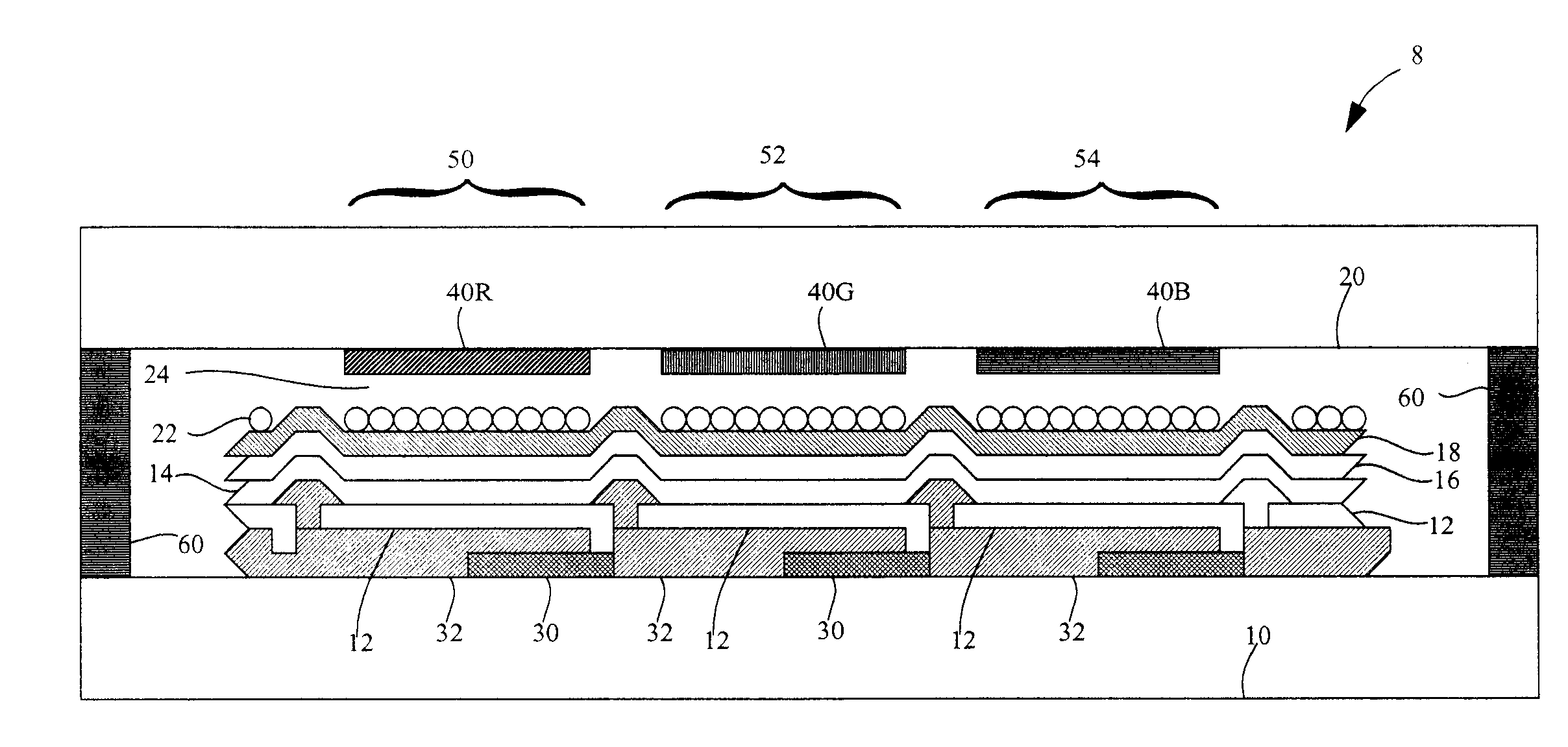
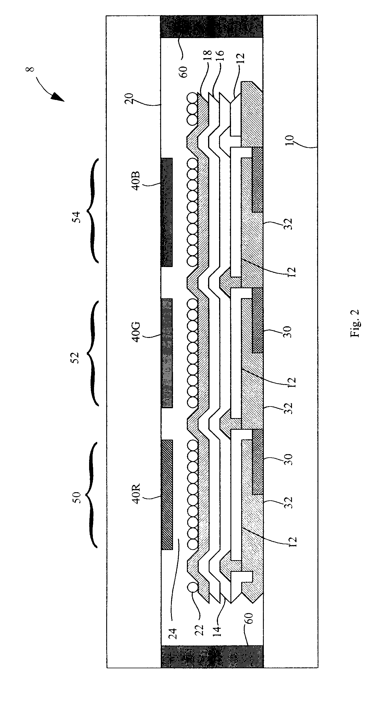
[0034]Referring to FIG. 1, a process for forming an OLED device, comprises the steps of providing 100 a substrate having a first electrode and one or more organic layers formed thereon, at least one organic layer being a light-emitting layer, forming 105 a conductive protective layer over the one or more organic layers opposite the first electrode by employing a vapor deposition process comprising alternately providing a first reactive gaseous material and a second reactive gaseous material, wherein the first reactive gaseous material is capable of reacting with the organic layers treated with the second reactive gaseous material, wherein the temperature of the gaseous materials and organic layers are less than 140 degrees C. while the gases are reacting and wherein the resistivity of the conductive protective layer is greater than 106 ohm per square; and forming 110 a second electrode over the conductive protective layer by sputter deposition. Because of the relatively high resista...


PUM

PropertyMeasurementUnit
internal pressureaaaaaaaaaa
thickaaaaaaaaaa
thicknessaaaaaaaaaa

Abstract

A process is disclosed for forming an OLED device, comprising: providing a substrate having a first electrode and one or more organic layers formed thereon, at least one organic layer being a light-emitting layer; forming a conductive protective layer over the one or more organic layers opposite the first electrode by employing a vapor deposition process comprising alternately providing a first reactive gaseous material and a second reactive gaseous material, wherein the first reactive gaseous material is capable of reacting with the organic layers treated with the second reactive gaseous material, wherein the temperature of the gaseous materials and organic layers are less than 140 degrees C. while the gases are reacting and wherein the resistivity of the protective layer is greater than 106 ohm per square; and forming a second electrode over the conductive protective layer by sputter deposition.

Description

FIELD OF THE INVENTION[0001]The present invention relates to organic light-emitting diode (OLED) devices, and more particularly, to a process for forming a conductive protective layer in an OLED device by vapor deposition.BACKGROUND OF THE INVENTION[0002]Organic light-emitting diodes (OLEDs) are a promising technology for flat-panel displays and area illumination lamps. The technology relies upon thin-film layers of organic materials coated upon a substrate. OLED devices generally can have two formats known as small-molecule devices such as disclosed in U.S. Pat. No. 4,476,292 and polymer OLED devices such as disclosed in U.S. Pat. No. 5,247,190. Either type of OLED device may include, in sequence, an anode, an organic EL element, and a cathode. The organic EL element disposed between the anode and the cathode commonly includes an organic hole-transporting layer (HTL), an emissive layer (EL) and an organic electron-transporting layer (ETL). Holes and electrons recombine and emit lig...

Claims


Application Information

Patent Timeline
Patent Type & Authority Applications(United States)
IPC IPC(8): H05B33/00H01L51/50
CPCC23C16/306C23C16/345C23C16/402C23C16/405H01L51/5237C23C16/45525C23C16/45555H01L51/5203C23C16/407H10K59/877H10K59/805H10K59/873H10K50/805H10K50/844H10K50/854
Inventor COK, RONALD S.
Owner EASTMAN KODAK CO
Features
  • Generate Ideas
  • Intellectual Property
  • Life Sciences
  • Materials
  • Tech Scout
  • Unparalleled Data Quality
  • Higher Quality Content
  • 60% Fewer Hallucinations
Learn More