Silicon light emitting diode, silicon optical transistor, silicon laser and its manufacturing method

a light-emitting diode and silicon technology, applied in the direction of lasers, semiconductor lasers, solid-state devices, etc., can solve the problems of low probability of such a phenomenon, high efficiency of silicon light-emitting diodes, and extremely poor light-emission efficiency of silicon, so as to achieve easy manufacturing and high efficiency

Inactive Publication Date: 2008-06-05
HITACHI LTD
View PDF16 Cites 40 Cited by
  • Summary
  • Abstract
  • Description
  • Claims
  • Application Information

AI Technical Summary

Benefits of technology

[0031]Of inventions to be disclosed in the present invention, the effect obtained by the representative invention will be briefly explained as follows:
[0032]According to the present invention, it becomes possible to provide a light-emitting device which can be easily fabricated on a substrate such as silicon by using the ordinary silicon process, and which can emit light with a high efficiency.

Problems solved by technology

However, it is difficult to cause silicon to emit light with a high efficiency, because silicon has the indirect-transition band structure.
Although it cannot be assured that the process like this does not exist physically, the probability is low that such a phenomenon will take place.
Consequently, it has been known that silicon, which is the indirect-transition semiconductor, exhibits an extremely bad light-emission efficiency.
As described above, silicon in the bulk state exhibits an extremely bad light-emission efficiency.
The laser formed of a compound semiconductor, however, is accompanied by the following problems: The material is the costly and expensive one, and implementation of the integration has been not developed.
The latter problem arises from the fact that the material is composed of a plurality of elements, and thus the control is difficult.
This is, e.g., the following problem: Assume that, when a single laser or light-receiving device is fabricated using a compound semiconductor, the yield has been found to be 70%.
In the case of the compound-semiconductor-used optical devices, however, implementation of the OEIC is difficult from the realistic point-of-view.
Consequently, there exists a problem that it is desired to implement a high-efficiency light-emitting device based on a IV semiconductor such as silicon or germanium comparable thereto.
However, the formation of silicon of the structure such as, e.g., the nano particles results in a feature that the silicon surface is extremely likely to be oxidized.
Accordingly, there exists a problem that the surface of the nano-particle silicon is oxidized to form silicon dioxide on the surface.
Since silicon dioxide is an insulating material whose bandgap is tremendously large, there occurs a problem that the formation of silicon dioxide on the surface prevents electrons and holes from being effectively injected.
Consequently, in the conventional silicon light-emitting devices, there occurs a problem that the light-emission efficiency is extremely lowered in electroluminescence even if high light-emission intensity can be obtained in photoluminescence.
However, there exists a problem that, in the nano particles formed by Chemical Vapor Deposition method or the structure that a large number of irregular holes are bored on the surface by anode oxidization, the crystalline property becomes worse as compared with the mono crystal.
The bad crystalline property gives rise to a situation that there occurs light emission with the intervention of a defect level.
The light emission using a defect is accompanied by a bad light-emission efficiency.
Accordingly, there exists a problem that it is impossible to manufacture a device which is practical and usable enough for the information communications and the like.
There exists a problem, however, that the light-emission efficiency has not attained to the practical level yet.
Consequently, there exists a problem that it is difficult to implement high-density integration of the devices in a manner compatible with the ordinary CMOS (Complementary Metal-Oxide-Semiconductor) technologies.
In order to integrate the silicon light-emitting devices on the same chip on which the LSIs, i.e., conventional electronic devices, are integrated, there exists a problem that it is desired to fabricate the silicon light-emitting devices by using a process which matches the conventional silicon process.
Accordingly, there exists a problem that it is desired to implement laser diodes by implementing laser oscillation.

Method used


Image

  • Silicon light emitting diode, silicon optical transistor, silicon laser and its manufacturing method
  • Silicon light emitting diode, silicon optical transistor, silicon laser and its manufacturing method
  • Silicon light emitting diode, silicon optical transistor, silicon laser and its manufacturing method

Examples


embodiment 1

[0115]In the present embodiment, the disclosure will be made below concerning a high-efficiency light-emitting device and a fabrication method of fabricating the high-efficiency light-emitting device. Here, the above-described light-emitting device is formed on a Silicon-On-Insulator (SOI) substrate by a method which allows the light-emitting device to be easily formed by using the ordinary silicon process.

[0116]FIG. 5A to FIG. 5H illustrate cross-sectional structures in the fabrication steps' sequence. Also, FIG. 6A to FIG. 6H illustrate schematic diagrams in the fabrication steps' sequence seen from the topside of a SOI substrate. Here, FIG. 5A to FIG. 5H are transverse-direction cross-sectional diagrams of FIG. 6A to FIG. 6H, respectively. For example, FIG. 5A illustrates a cross-sectional structure cut out by a cross section 13 in FIG. 6H (1). Also, FIG. 7 illustrates a schematic diagram of a cross-sectional structure cut out by a cross section 14 in FIG. 6H (1). FIG. 5H, FIG. 6...

embodiment 2

[0155]In the present embodiment, the disclosure will be made below concerning an optical interconnection and a fabrication method of fabricating the optical interconnection. Here, the above-described optical interconnection is based on information transmission performed by the light using the light-emitting device according to the first embodiment, which emits the light with a high efficiency on the chip using silicon or the like.

[0156]First, a silicon light-emitting diode is fabricated in accordance with fabrication steps similar to those in the first embodiment. In the silicon light-emitting diode in the present embodiment, width W of the extremely-thin silicon film is equal to 100 μm, and the length is equal to 100 μm. Also, simultaneously with the fabrication of the silicon light-emitting diode, a device illustrated on the upper side in FIG. 11 is fabricated in the region to which the ion implantation of the impurities has been not applied and in which the SOI layer has been not...

embodiment 3

[0170]In the present embodiment, the disclosure will be made below concerning a light-emitting field-effect transistor whose basic configuration element is a IV semiconductor, and whose light-emission intensity or light-emission wavelength is controllable with the gate voltage, and a fabrication method of fabricating the light-emitting field-effect transistor.

[0171]The light-emitting field-effect transistors according to the present embodiment can be easily integrated on a substrate such as silicon. Accordingly, the light-emitting field-effect transistors make it possible to configure a logic circuit using light.

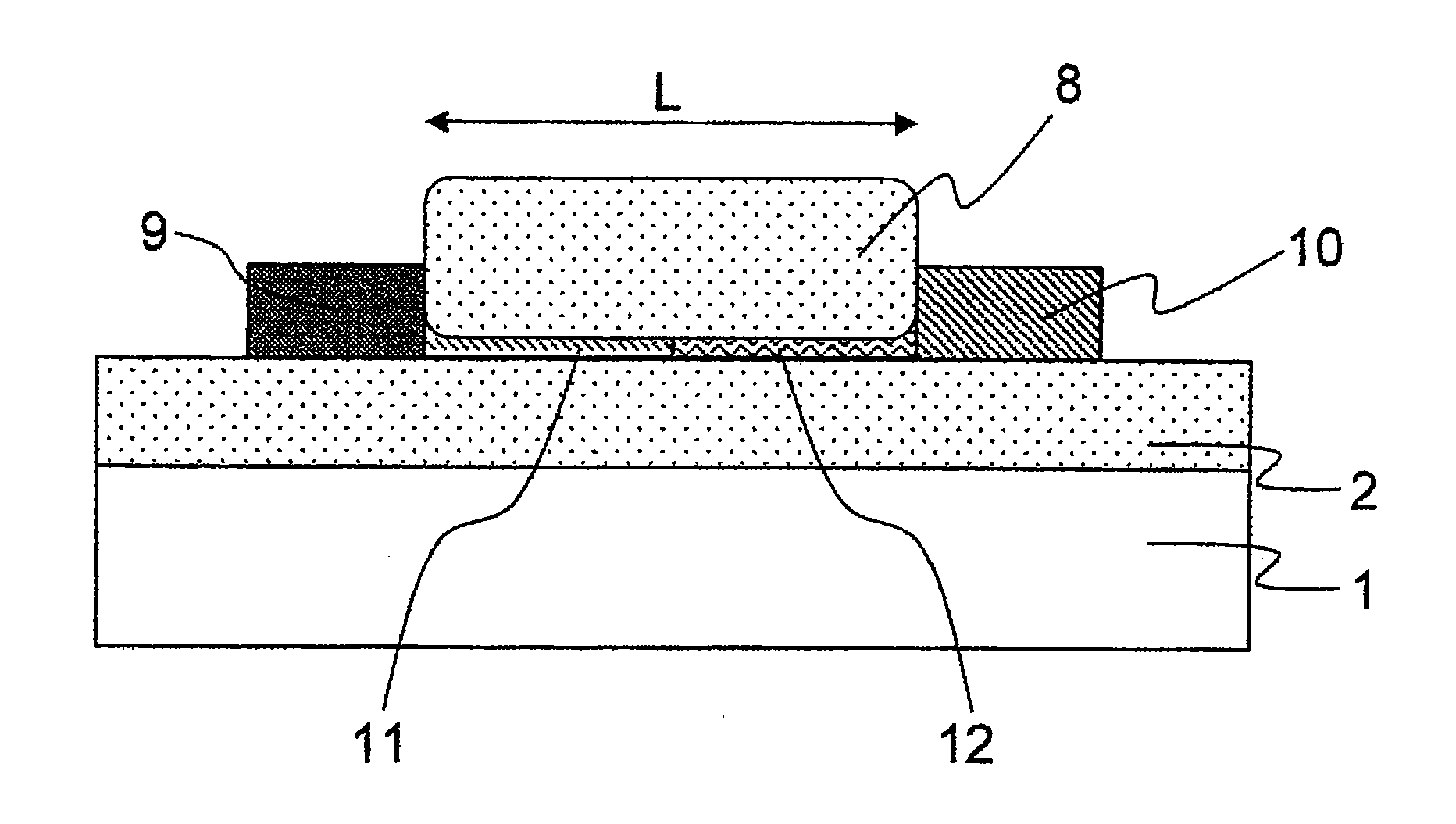
[0172]In the present embodiment, first, the silicon light-emitting diode is fabricated in accordance with fabrication steps similar to those in the first embodiment. Moreover, subsequently, silicon dioxide (not illustrated) attached on the surface of the silicon substrate 1 opposite to the surface adjacent to the BOX layer 2 is eliminated by being washed away using a solutio...


PUM


Abstract

A light-emitting device according to the present invention includes a first electrode unit 9 for injecting an electron, a second electrode unit 10 for injecting a hole, and light-emitting units 11 and 12 electrically connected to the first electrode unit 9 and the second electrode unit 10 respectively, wherein the light-emitting units 11 and 12 are formed of single-crystal silicon, the light-emitting units 11 and 12 having a first surface (topside surface) and a second surface (underside surface) opposed to the first surface, plane orientation of the first and second surfaces being set to a (100) plane, thicknesses of the light-emitting units 11 and 12 in a direction orthogonal to the first and second surfaces being made extremely thin.

Description

BACKGROUND OF THE INVENTION[0001]The present application claims priority from Japanese application JP-A-2006-120065 filed on Apr. 25, 2006, the content of which is hereby incorporated by reference into this application.FIELD OF THE INVENTION[0002]The present invention relates to a light-emitting device using silicon. More particularly, it relates to a high-luminance light-emitting diode, an optical transistor whose light intensity / wavelength is controllable with the gate voltage, a silicon laser, and their manufacturing method.DESCRIPTION OF THE RELATED ART[0003]In broadband networks which support the Internet industry, optical communications are employed. Lasers using III-V or II-VI compound semiconductors are used for light transmission / reception in the optical communications.[0004]Although various types of structures have been advocated for the compound semiconductor lasers, the most common one is the double hetero structure. The double hetero structure is a structure such that, ...

Claims


Application Information

Patent Timeline
Patent Type & Authority Applications(United States)
IPC IPC(8): H01L33/00H01L33/34
CPCH01S5/3224H01L33/34
Inventor SAITO, SHINICHIHISAMOTO, DIGHARAI, TADASHIONAI, TAKAHIRO
Owner HITACHI LTD
Why Eureka
Try Eureka