Depositing organic material onto an OLED substrate

a technology of organic material and substrate, which is applied in the direction of vacuum evaporation coating, solid-state devices, coatings, etc., can solve the problems of direct contact with the surface of the substrate, abrasion, distortion, or partial lifting of the first-color pattern, and difficult production, so as to achieve a larger oled display, easy to fabricate, and high material utilization

Inactive Publication Date: 2008-06-05
EASTMAN KODAK CO
View PDF10 Cites 120 Cited by
  • Summary
  • Abstract
  • Description
  • Claims
  • Application Information

AI Technical Summary

Benefits of technology

[0022]It is an advantage of this invention that the need for a precision two-dimensional mask is eliminated in the coating process, and that a linear mask, which is easier to fabricate, can be used. It is a further advantage of this invention that such a linear mask can have a major length much larger than practicable for a two-dimensional large-area mask, thus allowing the fabrication of larger OLED displays. It is a further advantage of this invention that it allows higher material utilization and less waste.

Problems solved by technology

The complexity of this process resides in the requirements that the integral shadow mask have multilevel topological features, which can be difficult to produce, and that angular positioning of the substrate with respect to one or more vapor sources must be controlled.
In general, positioning an element, such as a donor sheet or a mask, in direct contact with a surface of a substrate can invite problems of abrasion, distortion, or partial lifting of a relatively thin and mechanically fragile organic layer formed previously on the substrate surface.
In depositing a second-color pattern, direct contact of a donor sheet or a mask with the first-color pattern can cause abrasion, distortion, or partial lifting of the first-color pattern.
However, the ink-jet printing of dopants is performed under ambient conditions in which oxygen and moisture in the ambient air can result in partial oxidative decomposition of the uniformly deposited organic light-emitting layer containing the host material.
Additionally, direct diffusion of a dopant, or subsequent diffusion of a dopant, into the light-emitting layer can cause partial swelling and attendant distortion of the light-emitting layer.
This leads to poor material utilization factors and consequently high materials cost.
Although precision shadow-masking is a feasible method for OLED production, it also presents many potential complications to display manufacturing.
Second, when vacuum depositing on large-area substrates, it is difficult to keep shadow masks in intimate contact in all areas of the substrate, which can lead to unfocussed depositions or mask-induced physical damage to the substrate.
Third, when vacuum-depositing three colored regions at different locations on the substrate, three sets of precision shadow masks may be needed and can cause unwanted delays in OLED production.
Fourth, keeping mask-to-substrate precision alignment over the entirety of large substrates is very difficult for several reasons, including mask-substrate thermal expansion mismatches, small pixel pitches, and mask fabrication limitations.
Also, when vacuum depositing multiple substrates during a single vacuum pump-down cycle, material residue can build up on shadow masks and eventually cause defects to form in the pixels being deposited.

Method used


Image

  • Depositing organic material onto an OLED substrate
  • Depositing organic material onto an OLED substrate
  • Depositing organic material onto an OLED substrate

Examples


Embodiment Construction

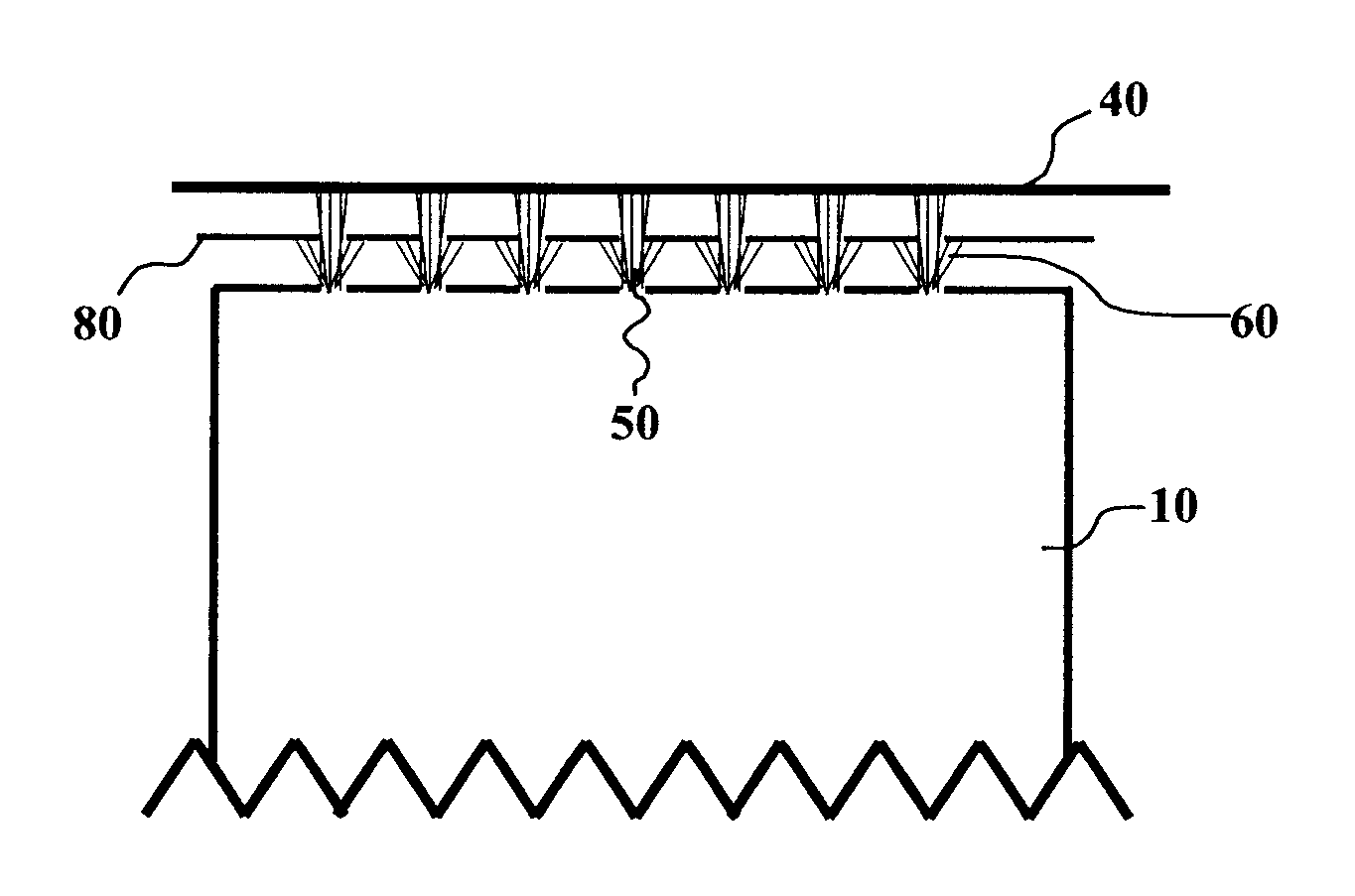
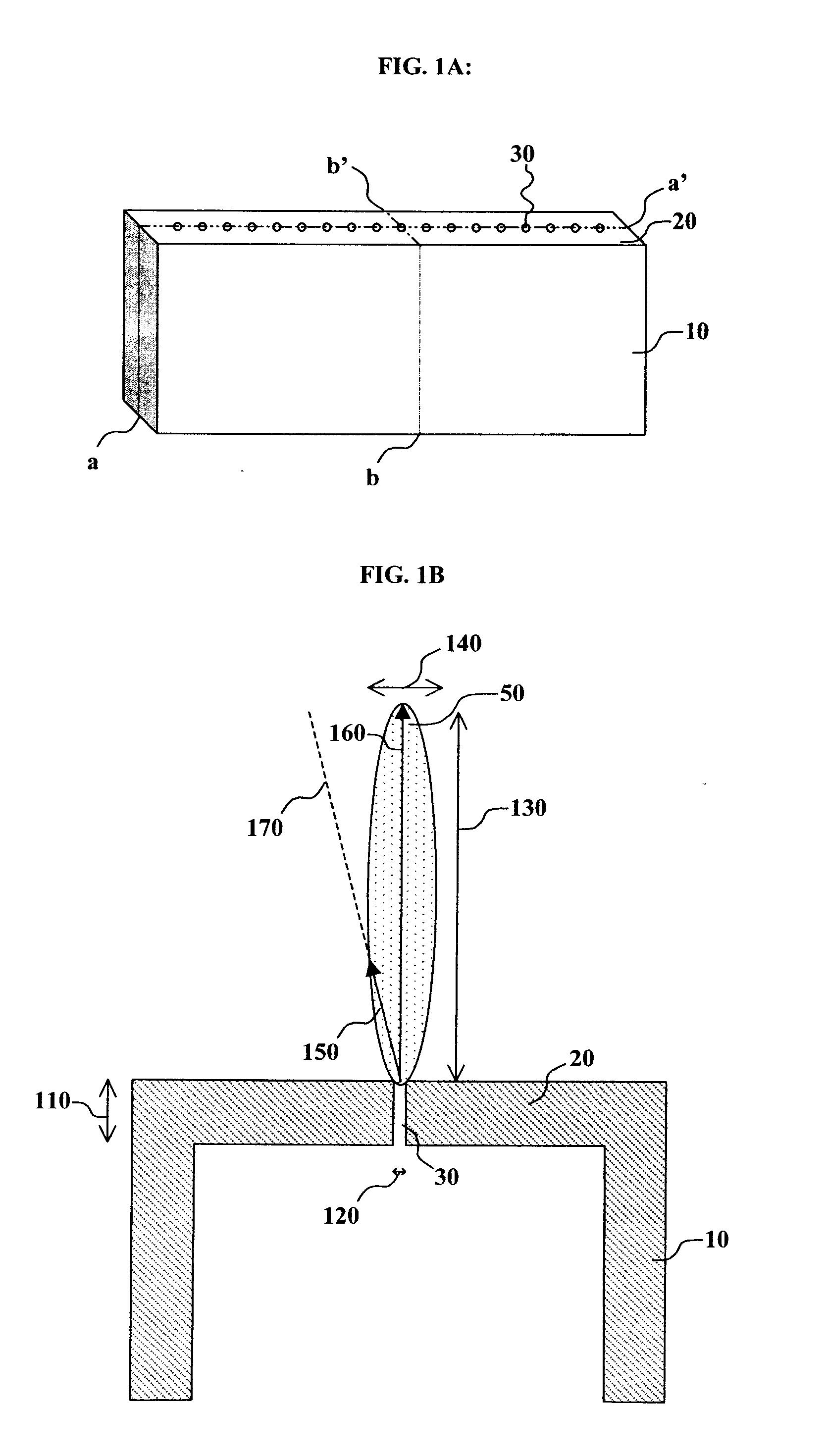
[0034]Turning now to FIG. 1A, there is shown one embodiment of a manifold with aperture plate openings that can be used in accordance with the method of this invention. Manifold 10 includes aperture plate 20, which has openings 30. As will be shown, openings 30 are selected so as to provide beams of vaporized organic material directed to a substrate. Manifold 10 can receive vaporized organic material that is provided by a variety of vaporization methods, such as those disclosed by Grace et al. in US Publication No. 2006 / 0099345, the contents of which are incorporated by reference. In one desirable embodiment, manifold 10 is an elongated manifold. That is, the length along section a-a′ is significantly greater than the width along section b-b′.

[0035]Manifold 10 and openings 30 are constructed so as to provide a directed beam of vaporized organic material under conditions of viscous flow or molecular flow. Turning now to FIG. 1B, there is shown one cross-sectional view of manifold 10 ...


PUM

PropertyMeasurementUnit
pressureaaaaaaaaaa
pressureaaaaaaaaaa
lengthaaaaaaaaaa

Abstract

A method of depositing organic material onto an OLED substrate, comprising: providing a manifold for receiving vaporized organic material, the manifold including an aperture plate having openings, the aperture plate openings being selected to provide beams of vaporized organic material directed to the substrate, such beams having off-axis components; and providing a mask spaced between the OLED substrate and the manifold, the mask having openings that respectively correspond to the aperture plate openings, the mask openings being selected to skim off at least a portion of the off-axis components of the beams.

Description

FIELD OF THE INVENTION[0001]The present invention relates to the field of physical vapor deposition on an OLED device where a source material is heated to a temperature so as to cause vaporization and form a thin film on a surface of a substrate.BACKGROUND OF THE INVENTION[0002]An organic light-emitting diode (OLED) device, also referred to as an organic electroluminescent device, can be constructed by sandwiching two or more organic layers between first and second electrodes.[0003]In single-color OLED devices or displays, also called monochrome OLEDs, these organic layers are not patterned but are formed as continuous layers. In multicolor OLED devices or displays or in full-color OLED displays, organic hole-injecting and hole-transporting layers are formed as continuous layers over and between the first electrodes. A pattern of one or more laterally adjacent organic light-emitting layers is then formed over the continuous hole-injecting and hole-transporting layer. This pattern, a...

Claims


Application Information

Patent Timeline
Patent Type & Authority Applications(United States)
IPC IPC(8): B05D5/06B05D1/32
CPCC23C14/042C23C14/12H01L51/56H01L51/0011H01L51/001H10K71/164H10K71/166H10K71/00
Inventor BOROSON, MICHAEL L.LONG, MICHAELGRACE, JEREMY M.REDDEN, NEIL P.WINTERS, DUSTIN L.PALONE, THOMAS W.
Owner EASTMAN KODAK CO
Why Eureka
Try Eureka