Conductive Ink

a technology of conductive ink and inkjet printing, which is applied in the direction of non-metal conductors, applications, conductors, etc., can solve the problems of inability to achieve the flat surface of the conductor surface, the inability to achieve multi-layer wiring, and the inability to use the conductive ink itself in the inkjet printing method. , to achieve the effect of reducing electric resistance, excellent adhesion and large features

Inactive Publication Date: 2008-06-12
MITSUI MINING & SMELTING CO LTD
View PDF7 Cites 56 Cited by
  • Summary
  • Abstract
  • Description
  • Claims
  • Application Information

AI Technical Summary

Benefits of technology

[0030]The conductive ink according to the present invention is suitable for forming accurate and fine wiring and electrode by adopting a dispenser coating method and an inkjet printing method. The conductive ink according to the present invention has excellent adhesion to a glass substrate and a circuit or the like formed by elements of different kinds. Therefore, the conductive ink enables the formation of the wiring, electrode, protection electrode and protection film on a gl...

Problems solved by technology

However, problems that the conductive ink itself hardly be used in the inkjet method or the adhesion strength of the conductive ink to the various substrates was extremely low were not solved.
On the other hand, even when the adhesion of the conductive ink to various substrates can be performed, the film density of the conductor circuit formed by using the conductive ink is low and the conductor resistance increase; thereby the heat generation inc...

Method used


Image

  • Conductive Ink
  • Conductive Ink
  • Conductive Ink

Examples


example 1

[0104]In this Example, a conductive ink was prepared by the following procedures; an electrode film was formed using the conductive ink; and the performances on the conductor resistance, adhesion and cross section of the electrode film were examined.

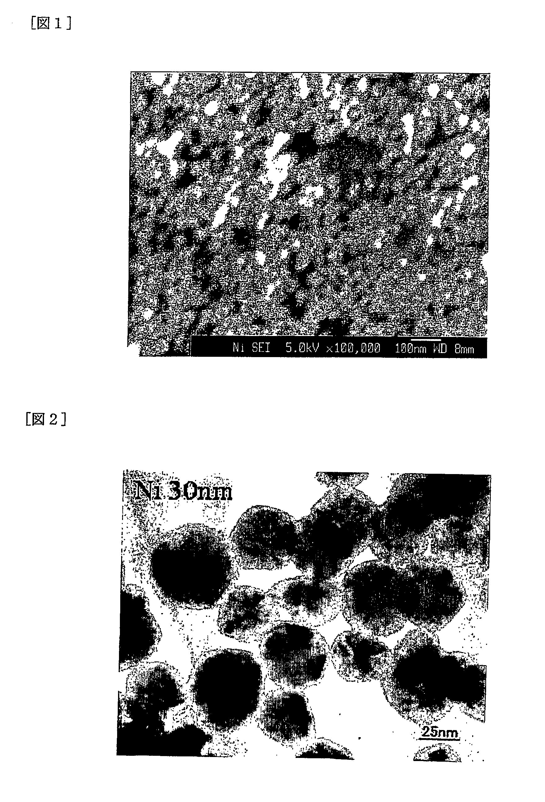
[0105]445.28 g of ethylene glycol in a reaction vessel charged with 31.31 g of nickel hydroxide, 2.15 g of polyvinylpyrrolidone (PVP), 0.69 ml of a 100 g / l palladium nitrate solution and 1.0 g of L-arginine was heated for 10 hours at 190 deg. C. while being stirred and nickel particles having an average primary particle size of 37.86 nano meter was obtained. This reaction solution was subjected to decantation using ethylene glycol to rinse and remove PVP contained in the reaction solution. Further, decantation was subjected twice using terpineol to produce a nickel slurry containing 80% by weight of nickel powder and terpineol as the balance.

[0106]Examination results on the primary particle size (average, standard deviation, maximum valu...

example 2

Preparation of Conductive Ink

[0114]In this Example, a conductive ink B was prepared in the same manner as in Example 1 except that citrate nickel is used as the film density improver to be added. Therefore, in order to avoid repeated description, the description of the manufacture process herein is omitted.

Measurement of Film Resistance:

[0115]Film of the above conductive ink B was formed on an alkali-free glass substrate OA-10 (manufactured by Nippon Electric Glass Co., Ltd.) by using a spin coater (manufactured by MIKASA Company) with 2500 rpm for 10 seconds. The specific resistance of the electrode film was 2.5×10⁻⁴ Ohm·cm, measured by a four-probe resistance measuring apparatus: RORESTER GP (manufactured by Mitsubishi Chemical Co., Ltd.).

Evaluation of Adhesion:

[0116]The adhesion of the electrode film to a glass substrate show good adhesion of class 0 when examined by a cross cut method according to JIS K 5600, paragraphs 5 to 6. On the electrode film prepared as described above a...

example 3

Preparation of Conductive Ink

[0118]In this Example, a conductive ink C was prepared in the same manner as in Example 1 except that copper acetate is used as the film density improver to be added. Therefore, in order to avoid repeated description, the description of the manufacture process herein is omitted.

Measurement of Film Resistance:

[0119]Film of the above conductive ink C was formed on an alkali-free glass substrate OA-10 (manufactured by Nippon Electric Glass Co., Ltd.) by using a spin coater (manufactured by MIKASA Company) with 2500 rpm for 10 seconds. The specific resistance of the electrode film was 5.92×10⁻⁴ Ohm·cm, measured by a four-probe resistance measuring apparatus: RORESTER GP (manufactured by Mitsubishi Chemical Co., Ltd.).

Evaluation of Adhesion:

[0120]The adhesion of the electrode film to a glass substrate show good adhesion of class 0 when examined by a cross cut method according to JIS K 5600, paragraphs 5 to 6. On the electrode film prepared as described above ...


PUM

PropertyMeasurementUnit
Viscosityaaaaaaaaaa
Surface tensionaaaaaaaaaa

Abstract

It is an object of the present invention to provide a conductive ink which enables to form a circuit or the like having excellent adhesion to a substrate and to form a conductor having high film density and low electric resistance. In order to attain the object, a conductive ink comprising metal powder or metal oxide powder dispersed in a dispersion medium, which is characterized in that the dispersion medium contains a metal salt or a metal oxide as a film density improver for increasing film density of a conductor formed by using the conductive ink is adopted. A main solvent constituting the dispersion medium is selected from one or a combination of two or more selected from the group consisting of water, alcohols, glycols and saturated hydrocarbons having a boiling point of 300 deg. C. or less at normal pressure.

Description

TECHNICAL FIELD[0001]The present invention relates to a conductive ink and a method for producing the same. In particular, the present invention relates to a conductive ink applicable to form a circuit on a substrate by drawing a circuit shape or the like by using, for example, inkjet method or the like followed by curing.BACKGROUND ART[0002]As methods for forming a circuit pattern on various substrates, a method which uses etching method with photolithography and a screen printing method have been conventionally applied as disclosed in Patent Documents 1 and 2. In these conventional methods, a method for subjecting a copper foil of a copper clad laminate to etching processing to form a circuit pattern, and a method for directly forming wiring and an electrode pattern on the surface of a substrate by screen printing using a conductive paste which is made to be paste by kneading metal powder with a solvent and a resin have been widely applied.[0003]A method to directly form a circuit...

Claims


Application Information

Patent Timeline
IPC IPC(8): C09D5/24B22F1/00B22F9/24B41J2/01B82Y10/00B82Y30/00B82Y40/00B82Y99/00C09D11/00C09D11/322C09D11/326C09D11/38C09D11/52C09K23/16C09K23/18C09K23/52H01B1/20H01B1/22H05K3/10
CPCC09D11/52H05K2201/0239H05K1/097H01B1/22B22F1/00
Inventor KAMIKORIYAMA, YOICHIOGATA, SUMIKAZUANAI, KEISAWAMOTO, HIROKIHORIUCHI, MIKIMASAMUKUNO, TAKASHIYOSHIMARU, KATSUHIKO
Owner MITSUI MINING & SMELTING CO LTD
Why Eureka
Try Eureka