Self-ionized and capacitively-coupled plasma for sputtering and resputtering

Active Publication Date: 2008-06-19
APPLIED MATERIALS INC
View PDF100 Cites 44 Cited by
  • Summary
  • Abstract
  • Description
  • Claims
  • Application Information

AI Technical Summary

Problems solved by technology

Lining and filling via holes and similar high aspect-ratio structures, such as occur in dual damascene, have presented a continuing challenge as their aspect ratios continue to increase.
Such a wide distribution can be disadvantageous for filling a deep and narrow via hole 122 such as that illustrated in FIG. 2, in which a barrier layer 124 has already been deposited.
Once a void 134 has formed, it is often difficult to reflow it out by heating the metallization to near its melting point.
Even a small void can introduce reliability problems.
If a second metallization deposition step is planned, such as by electroplating, the bridged overhangs make subsequent deposition more difficult.
Both long-throw targets and collimators typically reduce the flux of sputter particles reaching the wafer and thus tend to reduce the sputter deposition rate.
A yet further problem with both long throw and collimation is that the reduced metal flux can result in a longer deposition period which can not only reduce throughput, but also tends to increase the maximum temperature the wafer experiences during sputtering.
Still further, long-throw sputtering

Method used


Image

  • Self-ionized and capacitively-coupled plasma for sputtering and resputtering
  • Self-ionized and capacitively-coupled plasma for sputtering and resputtering
  • Self-ionized and capacitively-coupled plasma for sputtering and resputtering

Examples


Embodiment Construction

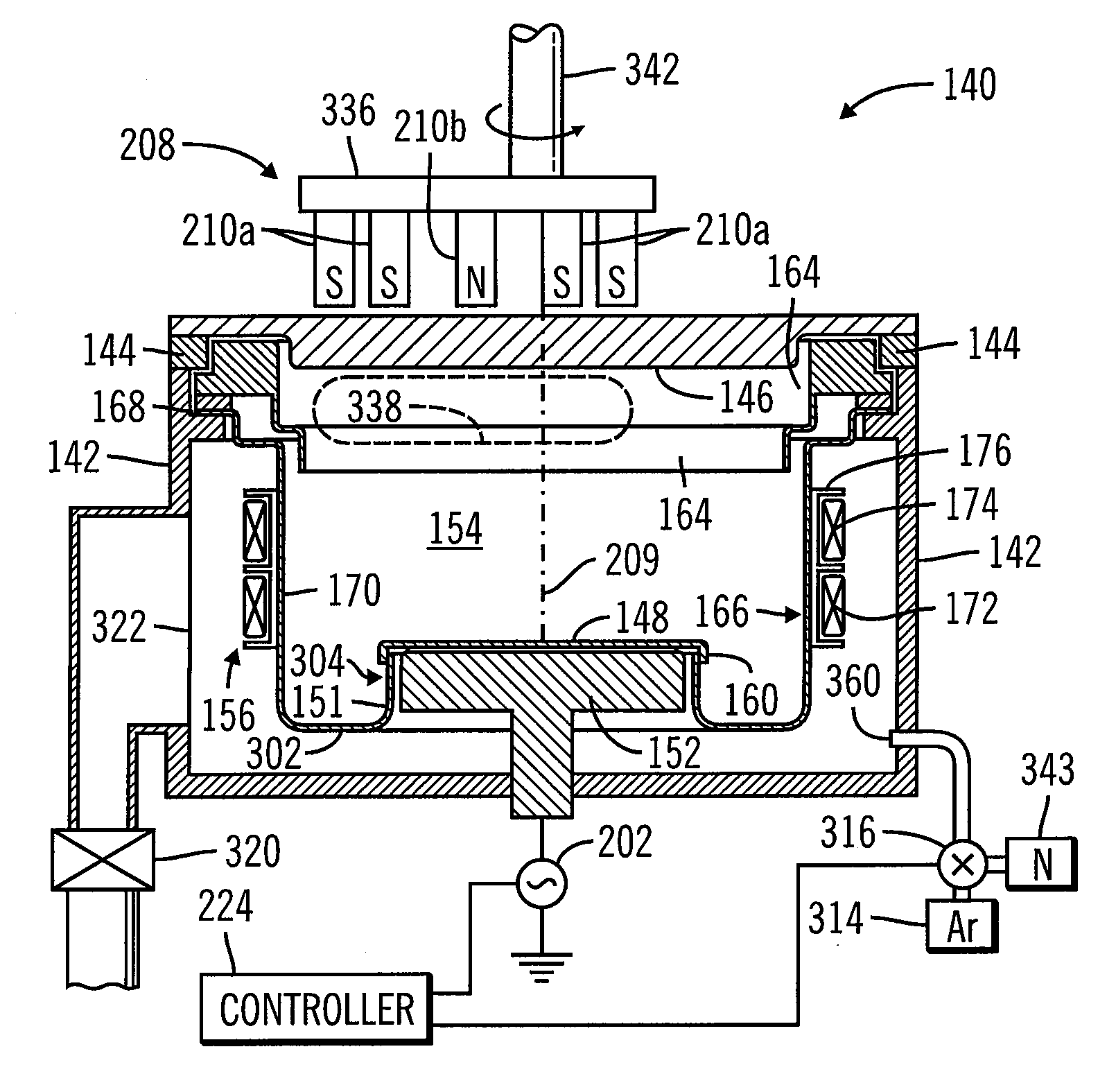
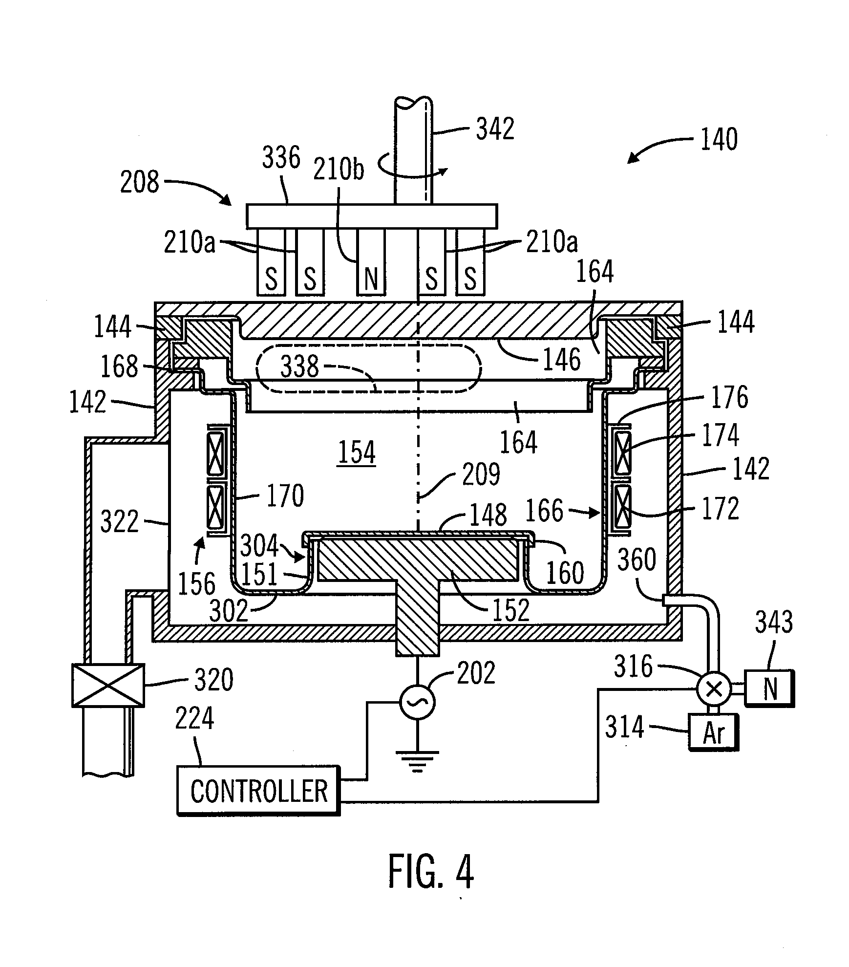
[0024]One embodiment of the present inventions is directed to sputter depositing a liner material such as tantalum or tantalum nitride, by combining long-throw sputtering, self-ionized plasma (SIP) sputtering and capacitively-coupled plasma (CCP) resputtering in one chamber. In a preferred embodiment, a magnetic field generated by an electromagnetic coil confines the plasma generated by capacitive coupling to increase the plasma density and hence the ionization rate. Long-throw sputtering is characterized by a relatively high ratio of the target-to-substrate distance to the substrate diameter. Long-throw SIP sputtering promotes deep hole coating of both the ionized and neutral deposition material components. CCP resputtering can reduce the thickness of layer bottom coverage of deep holes to reduce contact resistance.

[0025]SIP tends to be promoted by low pressures of less than 5 milliTorr. SIP, particularly at these low pressures, tends to be promoted by magnetrons having relatively ...


PUM

PropertyMeasurementUnit
Fractionaaaaaaaaaa
Diameteraaaaaaaaaa
Energyaaaaaaaaaa

Abstract

A DC magnetron sputter reactor for sputtering deposition materials such as tantalum and tantalum nitride, for example, and its method of use, in which self-ionized plasma (SIP) sputtering and capacitively coupled plasma (CCP) sputtering are promoted, either together or alternately, in the same chamber. Also, bottom coverage may be thinned or eliminated by inductively-coupled plasma (ICP) resputtering. SIP is promoted by a small magnetron having poles of unequal magnetic strength and a high power applied to the target during sputtering. CCP is provided by a pedestal electrode which capacitively couples RF energy into a plasma. The CCP plasma is preferably enhanced by a magnetic field generated by electromagnetic coils surrounding the pedestal which act to confine the CCP plasma and increase its density.

Description

RELATED APPLICATIONS[0001]This application is a continuation application of application Ser. No. 10 / 632,882 filed Jul. 31, 2003, which is incorporated by reference in its entirety. This application and application Ser. No. 10 / 632,882 claim the benefit of the U.S. Provisional Application No. 60 / 400,097 filed Aug. 1, 2002, which is incorporated by reference in entirety.FIELD OF THE INVENTION[0002]The inventions relate generally to sputtering and resputtering. In particular, the invention relates to the sputter deposition of material and resputtering of deposited material in the formation of semiconductor integrated circuits.BACKGROUND ART[0003]Semiconductor integrated circuits typically include multiple levels of metallization to provide electrical connections between large numbers of active semiconductor devices. Advanced integrated circuits, particularly those for microprocessors, may include five or more metallization levels. In the past, aluminum has been the favored metallization...

Claims


Application Information

Patent Timeline
IPC IPC(8): C23C14/14C23C14/34C23C14/35H01J37/34
CPCC23C14/345C23C14/35H01J37/3455H01J37/3408H01J37/32706
Inventor GOPALRAJA, PRABURAMFU, JIANMINGTANG, XIANMINFORSTER, JOHN C.KELKAR, UMESH
Owner APPLIED MATERIALS INC
Why Eureka
Try Eureka