Nanoholes and production thereof, stamper and production thereof, magnetic recording media and production thereof, and, magnetic recording apparatus and method
a technology of stamping and holes, applied in the field of nanohole structures, can solve the problems of increasing noise, decreasing magnetization, and nearing the limit of technology, and achieve the effects of low cost, high density, and efficient manufacturing
- Summary
- Abstract
- Description
- Claims
- Application Information
AI Technical Summary
Benefits of technology
Problems solved by technology
Method used
Image
Examples
example 1
Preparation of Nanohole Structure
[0251]A nanohole structure was prepared by the processes shown in FIGS. 9A to 9D. Initially, a resist layer 40 nm thick was formed on a glass substrate 52 by spin coating. A helical (spiral) line pattern was formed on the resist layer along a circumferential direction using a deep UV aligner (wavelength: 257 nm) to thereby form each of convex-and-concave patterns shown in Table 1. Each of the convex and concave patterns had an interval (pitch) between rows of concave portions of 1 mm and a depth of the rows of concave portions of 40 nm. A Ni layer was then formed on a surface of each convex and concave pattern by sputtering, the nickel layer as an electrode was subjected to electroforming in a nickel sulfamate bath to a thickness of the nickel layer of 0.3 mm, and the backside of the substrate was polished to thereby yield a series of Ni stamper molds 51 (FIG. 9A; mold preparation process).
[0252]Next, each of the above-prepared Ni stamper molds was p...
example 2
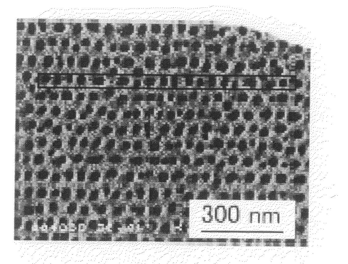
[0255]A mold was prepared by the procedure of Example 1, except for using an electron beam (EB) aligner instead of the deep UV aligner and for forming a helical pattern 60 nm wide of rows of concave portions at intervals (pitch) between rows of 100 nm. Separately, an aluminum layer 100 nm thick was formed by sputtering on a magnetic disk substrate made of silicon. The above-prepared mold was pressed to the aluminum layer to thereby imprint and transfer the pattern to the aluminum layer. The aluminum layer was then anodized at a voltage of 40 V in a diluted sulfuric acid solution to thereby form rows of nanoholes in which nanoholes (alumina pores) were spaced in rows at specific intervals on the rows of concave portions. Then, cobalt (Co) 56 was charged into individual nanoholes (alumina pores) in the rows of nanoholes by electrodeposition (FIG. 9E; magnetic meal electrodeposition process). The resulting article was observed by a scanning electron microscope to find to have a structu...
example 3
[0256]The procedure of Example 2 was repeated except that the pattern of the rows of concave portions was partitioned by a length of 500 nm in its longitudinal direction (FIG. 12A; mold). As a result, five nanoholes (alumina pores) were formed at substantially equal intervals in every partitioned region 500 nm long of the rows of concave portions (FIG. 12B; after electrodeposition of Co). The result shows that nanoholes (alumina pores) can be formed in a specific number in a more regular array by partitioning the pattern of the rows of concave portions at specific intervals, as compared with a continuous pattern of the rows of concave portions.
PUM
| Property | Measurement | Unit |
|---|---|---|
| thickness | aaaaa | aaaaa |
| thickness | aaaaa | aaaaa |
| thickness | aaaaa | aaaaa |
Abstract
Description
Claims
Application Information


