Transparent conductive film and method for producing the same

Inactive Publication Date: 2008-07-10
NITTO DENKO CORP
View PDF3 Cites 27 Cited by
  • Summary
  • Abstract
  • Description
  • Claims
  • Application Information

AI Technical Summary

Benefits of technology

[0025]A transparent conductive film can be produced by forming a ZnO-based thin film, such as a GZO thin film made of Ga-doped ZnO and an AZO thin film made of Al-doped ZnO, directly on an organic polymer film substrate. In this case, if the thickness of the ZnO-based thin film is increased to 200 nm or more, the crystal can grow along the c axis to have a low resistance value so that the rate of resistance change can be low even in a hot and humid environment. Thus, the properties such as resistance to moisture and heat can be significantly improved. On the other hand, although the substrate temperature is low, the ZnO-based thin film with a thickness of about 150 nm or less cannot show sufficient crystal growth along the c axis, has a high resistance value, exhibits a high rate of resistance change also in a hot and humid environment, and thus is very poor in resistance to moisture and heat.
[0026]In the transparent conductive film of the invention, the ZnO-based thin film is formed on the organic polymer film substrate with the Al2O3 thin film interposed therebetween, so that the ZnO-based thin film even with a thickness of 150 nm or less can satisfy a low resistance value, exhibit a low rate of resistance change even in a hot and humid environment, and have good resistance to moisture and heat.
[0027]For example, when the Al2O3 thin film is provided between the organic polymer film substrate and the ZnO-based thin film, the resistance of the ZnO-based thin film is lower than that of the ZnO-based thin film formed with the same thickness directly on the organic polymer film substrate. When the ZnO-based thin film is a GZO thin film, the resistance is reduced by 20 to 50%. Particularly when the GZO film is produced from Zn—Ga as a metal target, the rate of the reduction in the resistance value is high. When the ZnO-based thin film is an AZO thin film, the resistance is reduced by about 30%. When the ZnO-based thin film is formed on the Al2O3 thin film (not directly on the organic polymer film substrate), the ZnO-based thin film increases in both mobility (μ) and carrier density (n). Thus, it can be considered that the ZnO-thin film has the crystal orientation aligned to the c axis to form a strongly c-axis oriented crystal film so that it can have improved low resistance and improved resistance to mois

Problems solved by technology

At present, the dominating transparent electrode materials are ITO (In—Sn complex oxide) thin films, but In, a main component of ITO, has a depletion problem.
However, organic polymer film substrates can only be heated to 180° C. or less.
However, the resulting thin films are polycrystalline and low in both mobility (u) and carrier density (n).
When the crystal films are subjected to a heating and humidifying test and then examined for resistance change, their specific resistance is higher than that of thick films with a thickness of 200 nm or more, and there is a problem in which only films whose resistance is extremely changed by the heating and humidifying test are obtainable (Proceedings of the 67th Meeting of the J

Method used


Image

  • Transparent conductive film and method for producing the same
  • Transparent conductive film and method for producing the same
  • Transparent conductive film and method for producing the same

Examples


examples

[0078]The invention is described below with reference to some examples which are not intended to limit the scope of the invention.

[0079]The invention is more specifically described by showing the examples below which are not intended to limit the scope of the invention.

examples 1

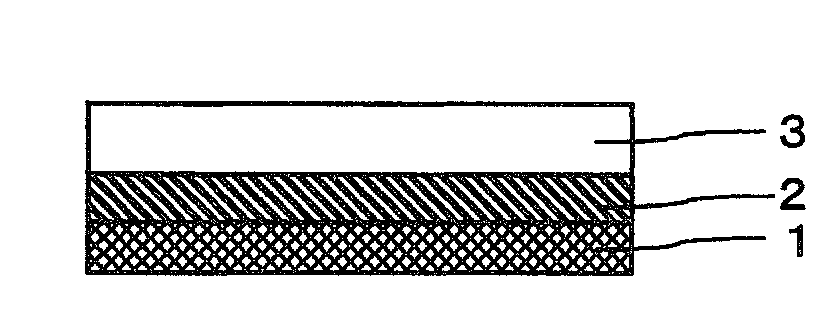
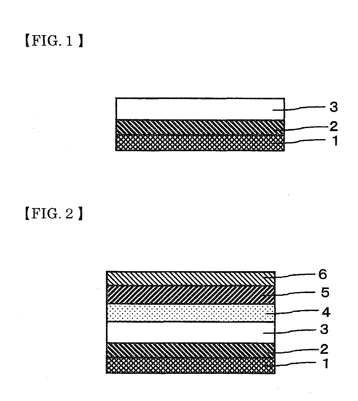
Organic Polymer Film Substrate

[0080]The organic polymer film substrate used was a polyethylene terephthalate (PET) film 0300E (100 μm in thickness) manufactured by Mitsubishi Plastics Inc.

Pretreatment

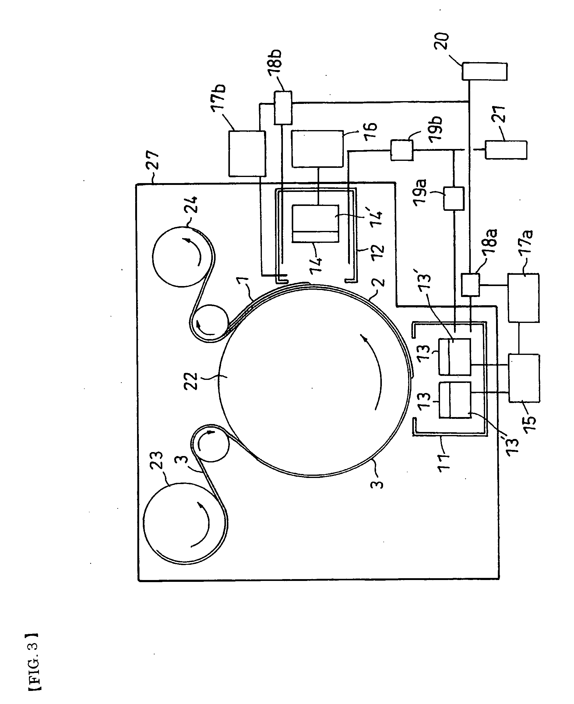
[0081]The PET film was placed in a sputter deposition device as shown in FIG. 3 such that an Al2O3 thin film was able to be formed on its smooth surface (not undergoing smoothing treatment) of the PET film. The roller electrode used was heated to 120° C. While the film was wound, degassing was performed with an evacuation device including a cryocoil and a turbopump so that an ultimate vacuum of 1.5×10⁻⁶ Pa was achieved. Argon gas was then introduced, and the film was allowed to pass through plasma discharge at 13.56 MHz so that the PET surface was pretreated.

Formation of Al2O3 Thin Film

Undercoat Layer

[0082]Al as a target was then mounted on each electrode of the dual magnetron sputtering device of FIG. 3. While argon gas was introduced at 150 sccm (air-equivalent gas flow rate, cc / minut...

example 2

[0084]A transparent conductive film was obtained in the same manner as in example 1, except that the GZO thin film was formed by the method described below.

Formation of GZO Thin Film

[0085]The target for producing the GZO thin film was replaced with ZnO-5.7% by weight Ga2O3 (ZnO—Ga2O3 with a Ga2O3 content of 5.7% by weight) as an oxide target, and the film was formed under only argon gas with a DC power of 3 kw. The amount of the introduction of the argon gas was 300 sccm, and the film was produced under a pressure of 0.3 Pa. The GZO thin film had a thickness of about 40 nm.


PUM

PropertyMeasurementUnit
Temperatureaaaaaaaaaa
Thicknessaaaaaaaaaa
Pressureaaaaaaaaaa

Abstract

A transparent conductive film comprising: an organic polymer film substrate; an Al2O3 thin film formed on the organic polymer film substrate; and a ZnO-based thin film that is formed on the Al2O3 thin film and comprises ZnO doped with at least one of Ga and Al. The transparent conductive film has a low resistance value, even when the thickness of the ZnO-based thin film is reduced (particularly to about 150 nm or less), and shows a low rate of resistance change even in a hot and humid environment.

Description

BACKGROUND OF THE INVENTION[0001]1. Field of the Invention[0002]The present invention relates to a transparent conductive film and a method for producing the same. For example, the transparent conductive film of the invention may be used in electrode applications such as transparent electrodes for touch panels and electrodes for film solar cells and other applications including transparent electrodes for advanced display devices such as liquid crystal displays and electroluminescent displays and electromagnetic wave shielding or prevention of static charge of transparent products.[0003]2. Description of the Related Art[0004]Recently, demanded types of touch panels, liquid crystal display panels, organic electroluminescent (OLED) panels, electrochromic panels, electronic paper devices, and so on are being changed from conventional devices using transparent electrode-attached glass substrates to devices using film substrates in which transparent electrodes are provided on transparent ...

Claims


Application Information

Patent Timeline
IPC IPC(8): B05D5/12B32B9/00C23C14/34
CPCC23C14/0042Y10T428/265C23C14/086C23C14/081C08J5/18G02F1/1335
Inventor SASA, KAZUAKIKAWAMURA, KAZUNORI
Owner NITTO DENKO CORP
Why Eureka
Try Eureka