Reflective mask blank for EUV lithography

a lithography and mask technology, applied in the field of reflection mask blanks, can solve the problems of accelerating microsizing of semiconductor devices, close to the resolution limit of conventional photolithography, etc., and achieve the effects of low electrical resistivity, excellent smoothness, and high electrical resistan

Inactive Publication Date: 2008-07-31
ASAHI GLASS CO LTD
View PDF24 Cites 24 Cited by
  • Summary
  • Abstract
  • Description
  • Claims
  • Application Information

AI Technical Summary

Benefits of technology

[0043]In the EUV mask blank of the present invention, the absorber layer comprises Hf having a low electrical resistivity, and accordingly, it is free from deterioration of the film deposition rate during the film deposition for the absorber layer and free from instability of the discharge during the film deposition, which may occur in the case where the absorber layer has high electrical resistance and the absorber layer contains insulating B (boron). Accordingly, there will be no such problem that the film composition or the film thickness fluctuates at the time of forming the absorber layer or further that the film deposition becomes impossible.
[0044]In the EUV mask blank of the present invention, the crystalline state of the absorber layer is amorphous, and the absorber surface is excellent in smoothness. As a result, there will be no such a trouble that the edge roughness of a pattern formed in the absorber layer becomes large or that the dimensional precision of the pattern deteriorates.
[0045]Further, the absorber layer has characteristics excellent for an EUV mask blank, such that the reflectance against EUV light and the reflectance against light within a wavelength region of light to be used for inspection of a pattern, are low.
[0046]Further, the absorber layer comprising Ta and Hf has an etching rate higher than a TaBN film, whereby an effect to reduce the damage to the resist during etching, is expected.
[0047]Further, by such reduction of the damage to the resist, it is expected that the film thickness of the resist can be reduced.
[0048]Further, the content of nitrogen in the absorber layer is preferably 0 to at most 35 at. %, whereby the crystalline state of the absorber layer tends to readily be amorphous, the light reflectance in the wavelength region of light for inspection of a pattern can be made low, the etching rate can be made high, and an increase in electrical resistivity can be suppressed.

Problems solved by technology

However, the conventional photolithography method has been close to the resolution limit, while microsizing of semiconductor devices has been accelerated.

Method used


Image

  • Reflective mask blank for EUV lithography
  • Reflective mask blank for EUV lithography

Examples


example 1

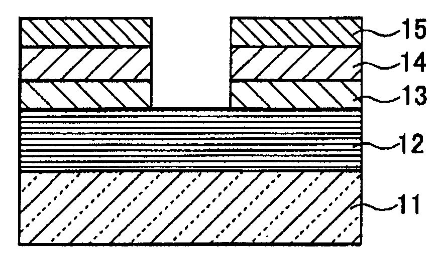
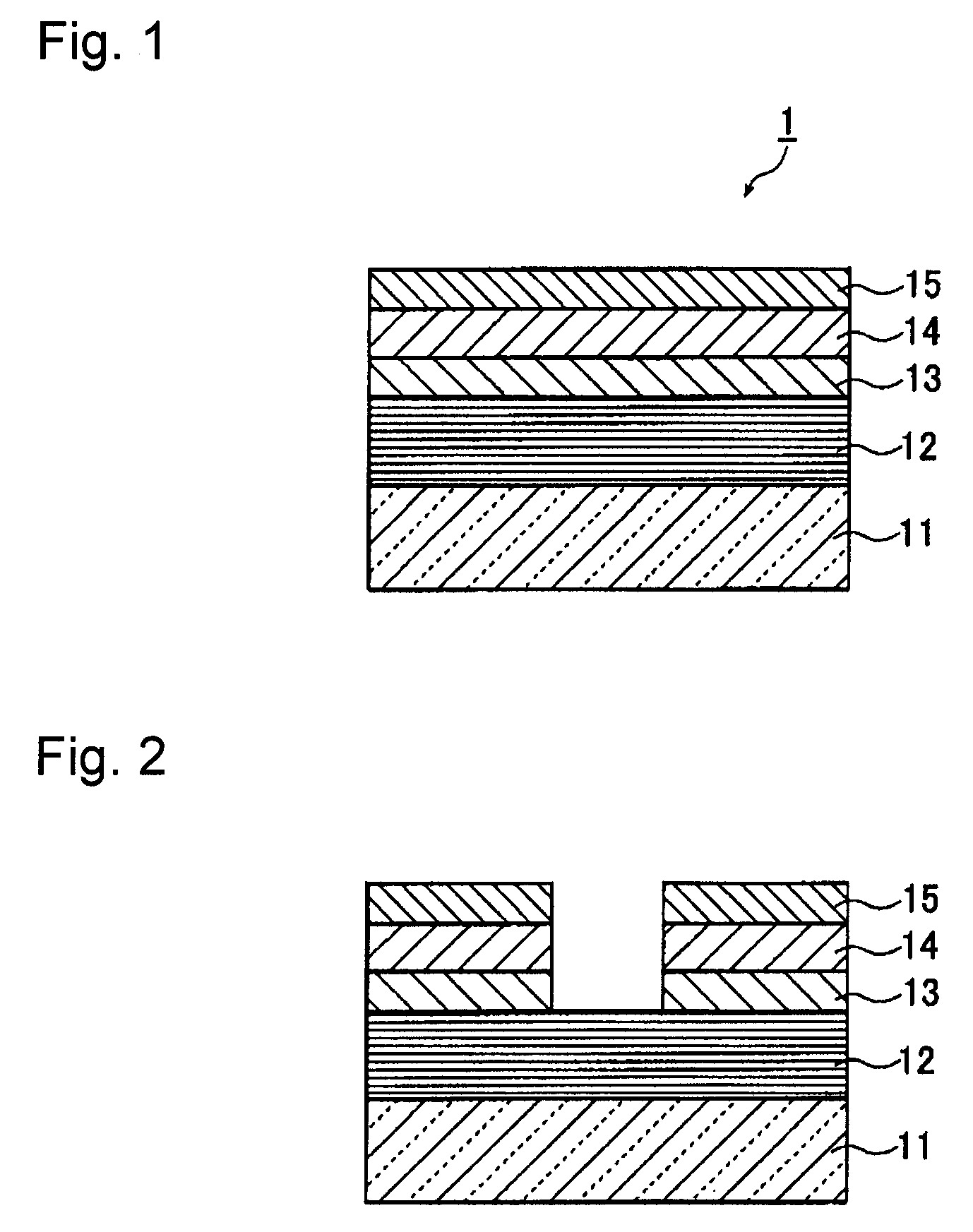
[0144]In this Example, an EUV mask blank 1 shown in FIG. 1 was prepared. However, in the EUV mask blank 1 in Example 1, a low reflective layer 15 was not formed on an absorber layer 14. As a substrate 11 for film deposition, a SiO2—TiO2 glass substrate (size: 6 inch (152 mm) square, thickness: 6.3 mm) was used. This glass substrate has a thermal expansion coefficient of 0.2×10⁻⁷ / ° C., a Young's modulus of 67 GPa, a Poisson ratio of 0.17 and a specific rigidity of 3.07×10⁷ m2 / s2. This glass substrate was formed by polishing to have a smooth surface with a surface roughness (rms) of at most 0.15 nm and to a flatness of at most 100 nm.

[0145]On the rear side of the substrate 11, a Cr film having a thickness of 100 nm was deposited by means of magnetron sputtering to provide a high dielectric coating having a sheet resistance of 100Ω / □.

[0146]To a flat plate-shaped usual electrostatic chuck, the substrate 11 (size: 6 inch (152 mm) square, thickness: 6.3 mm) was fixed by means of the forme...

example 2

[0181]In this Example, an EUV mask blank 1 was prepared wherein a low reflective layer 15 (TaHfON film) containing Ta, Hf, O and N is formed on an absorber layer 14.

[0182]In this Example, the procedure to form an absorber layer 14 on a protective layer 13 was carried out in the same manner as in Example 1. On the absorber layer 14, a low reflective layer (TaHfON film) containing Ta, Hf, O and N was formed by magnetron sputtering, as a low reflective layer 15 against an inspection light having a wavelength of 257 nm. The compositional ratio (at. %) of the low reflective layer was measured by the same method as in Example 1 and found to be Ta:Hf:N:O=35:15:15:35.

[0183]The film deposition conditions for the low reflective layer 15 (TaHfON film) were as follows.

Film Deposition Conditions for Low Reflective Layer 15 (Tahfon Film)

[0184]Target: TaHf compound target (compositional ratio: Ta 55 at. %, Hf 45 at. %)

[0185]Sputtering gas: Mixed gas of Ar, N2 and O2 (Ar: 45 vol %, N2: 23 vol %, O2...

example 3

[0232]In this Example, an EUV mask blank 1 was prepared wherein a low reflective layer 15 (TaHfO film) containing Ta, Hf and O was formed on an absorber layer 14.

[0233]In this Example, the procedure up to forming an absorber layer 14 on a protective layer 13 was carried out in the same manner as in Example 1. On an absorber layer 14, a low reflective layer (TaHfO film) containing Ta, Hf and O was formed by magnetron sputtering as a low reflective layer 15 against an inspection light having a wavelength of 257 nm. The compositional ratio (at. %) of the low reflective layer was measured in the same manner as in Example 1 and found to be Ta:Hf:O=40:20:40.

[0234]The film deposition conditions for the low reflective layer 15 (TaHfO film) were as follows.

Film Deposition Conditions for Low Reflective Layer 15 (TaHfO FILM)

[0235]Target: TaHf compound target (compositional ratio: Ta 55 at. %, Hf 45 at. %)

[0236]Sputtering gas: Mixed gas of Ar and O2 (Ar: 70 vol %, O2: 30 vol %, gas pressure: 0....


PUM

PropertyMeasurementUnit
surface roughnessaaaaaaaaaa
thicknessaaaaaaaaaa
thicknessaaaaaaaaaa

Abstract

To provide a reflective mask blank for EUV lithography having an absorber layer which has a low reflectance in a wavelength region of EUV light or light for inspection of a pattern and which is easy to control to have a desired layer composition and thickness.
A reflective mask blank for EUV lithography, which comprises a substrate, and a reflective layer to reflect EUV light and an absorber layer to absorb EUV light, formed in this order on the substrate, wherein the absorber layer contains tantalum (Ta) and hafnium (Hf), and in the absorber layer, the content of Hf is from 20 to 60 at. % and the content of Ta is from 40 to 80 at. %, and wherein the absorber layer has a content of N being 0 to at most 35 at. %.

Description

TECHNICAL FIELD[0001]The present invention relates to a reflective mask blank (in this specification, hereinafter referred to as “EUV mask blank”) for EUV (Extreme Ultra Violet) lithography to be used for e.g. production of semiconductors.BACKGROUND ART[0002]In the semiconductor industry, a photolithography method using visible light or ultraviolet light has been employed as a technique for writing, on a Si substrate or the like, a fine pattern, which is required for forming an integrated circuit comprising such a fine pattern. However, the conventional photolithography method has been close to the resolution limit, while microsizing of semiconductor devices has been accelerated. In the case of the photolithography method, it is said that the resolution limit of a pattern is about ½ of an exposure wavelength, and that even if an immersion method is employed, the resolution limit is about ¼ of an exposure wavelength. Even if an immersion method using an ArF laser (193 nm) is employed...

Claims


Application Information

Patent Timeline
Patent Type & Authority Applications(United States)
IPC IPC(8): G03F1/00G03F7/26G03F1/24G03F1/46G03F1/58
CPCG03F1/14G03F1/58G03F1/46G03F1/24
Inventor HAYASHI, KAZUYUKIKADOWAKI, KAZUOSUGIYAMA, TAKASHI
Owner ASAHI GLASS CO LTD
Why Eureka
Try Eureka