

CMOS image sensor chip scale package with die receiving opening and method of the same
- Summary
- Abstract
- Description
- Claims
- Application Information
AI Technical Summary
Benefits of technology
Problems solved by technology
Method used
Image

Examples
Embodiment Construction
[0018]The invention will now be described in greater detail with preferred embodiments of the invention and illustrations attached. Nevertheless, it should be recognized that the preferred embodiments of the invention is only for illustrating. Besides the preferred embodiment mentioned here, present invention can be practiced in a wide range of other embodiments besides those explicitly described, and the scope of the present invention is expressly not limited expect as specified in the accompanying claims.
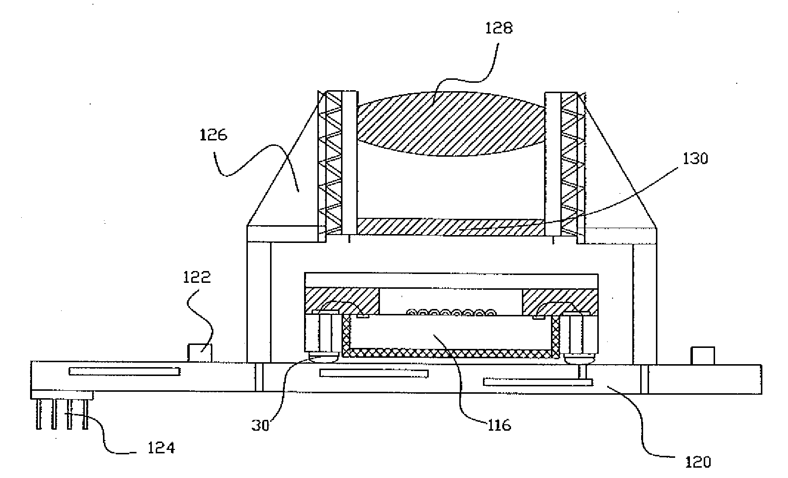
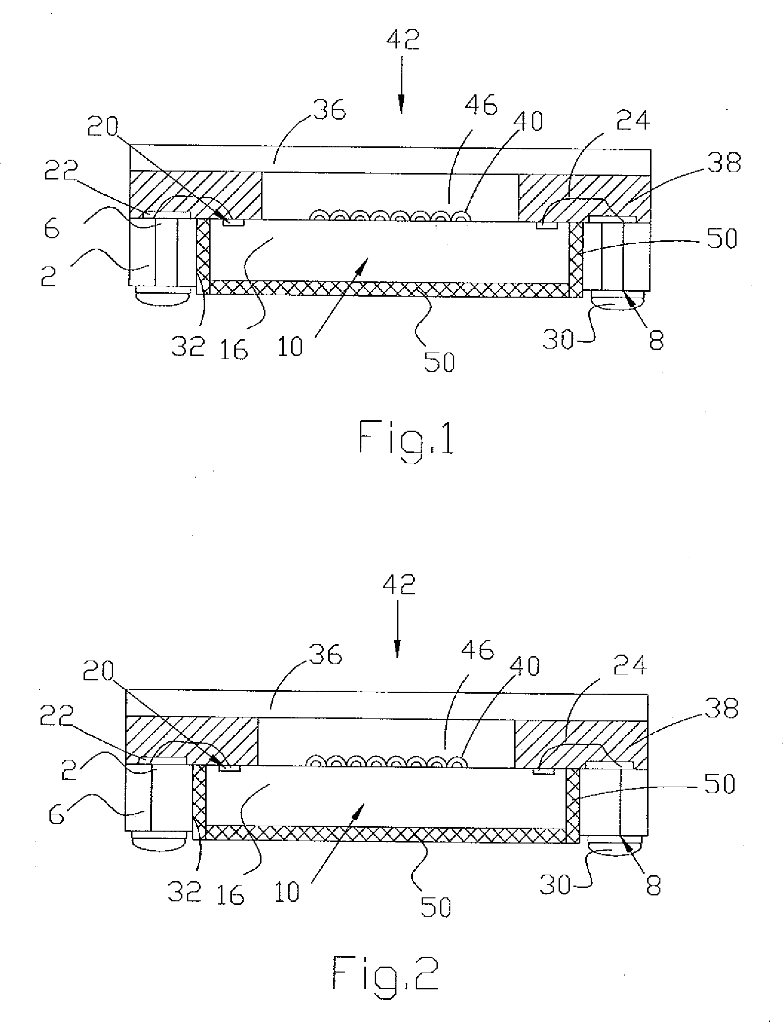
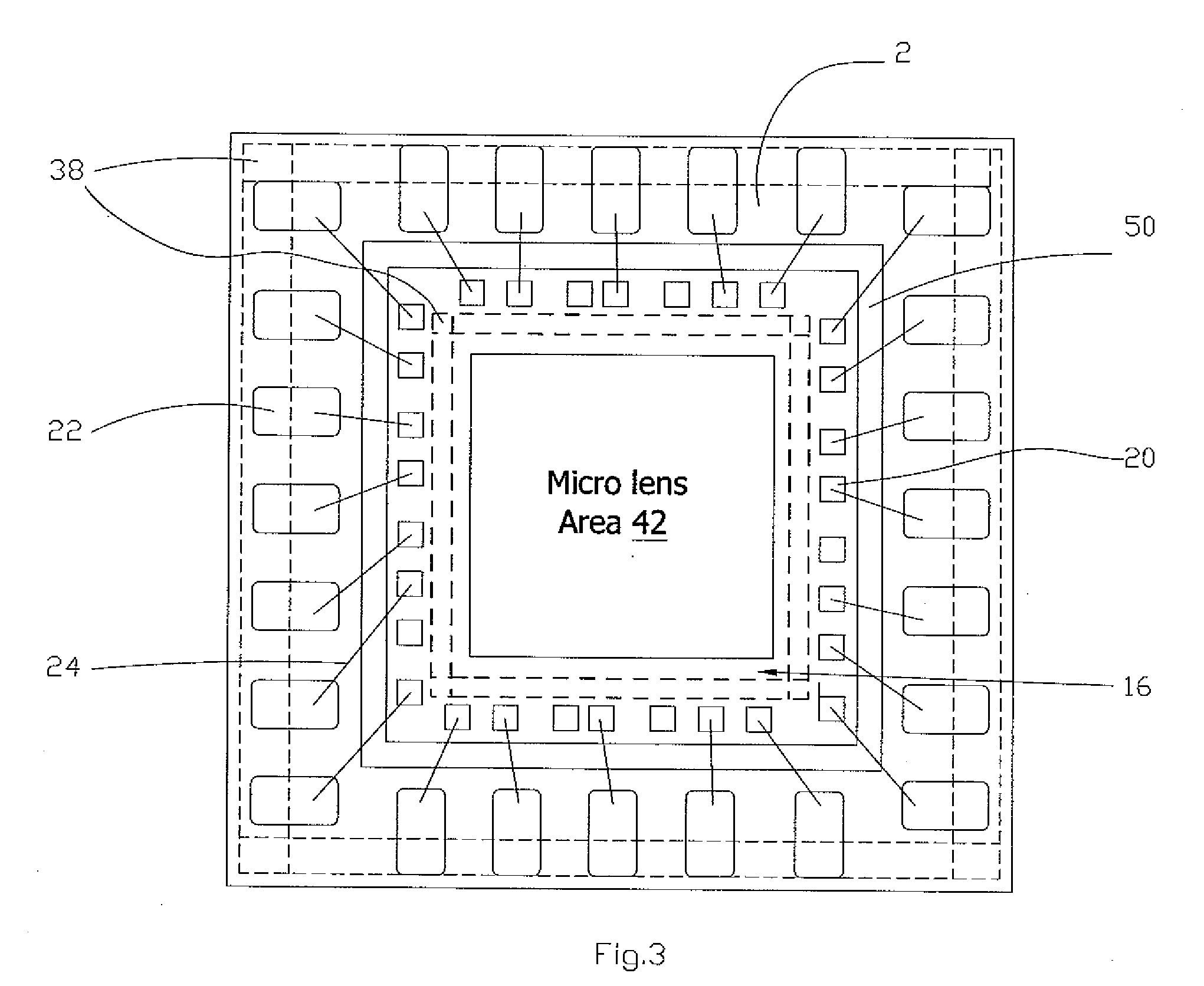
[0019]The present invention discloses a structure of Panel Level Package (PLP) utilizing a substrate having predetermined die through holes and contact (inter-connecting) through holes formed, and the contact metal pads on the upper side and the terminal metal pads on the lower side through the metal of through holes therein and a plurality of openings passing through the substrate. A wire bonding is connected between pads formed on an image sensor die and contact metal pads of th...
PUM
 Abstract
Description
Claims
Application Information