[0014]The present invention is a method of making a diffusion-impeding barrier layer, also known as interfacial layer (IFL), within a photovoltaic
cell comprising, for example, cadmium
telluride,
cadmium sulfide, and a metal-comprising electrical contact, by exposing the surface of the cadmium telluride layer to a
halogen (e.g., fluorine) to create a Te-poor cadmium
fluoride barrier layer. The present invention is not limited to
copper and will work for any metal electrical contact metal, as well as any material comprising any a
Group II-VI element, including but not limited to CuInGaSe photovoltaic material, also known as CIGS. Although specific reference is made to CdTe
photovoltaics, the invention is not limited thereto. A skilled artisan will appreciate that virtually any photovoltaic material can benefit from the teachings herein. By inhibiting metal diffusion and maintaining the integrity of the electrical contact, these compounds increase the efficiency and serviceable lifetime of a photovoltaic.
[0015]For example, the present invention provides a more thermally stable, low-resistance contact on a p-type CdTe photovoltaic cell by forming a Te-poor barrier layer of CdF2, which is a more thermodynamically stable compound than CdTe, Cu2Te, or CuTe, by exposing the p-type layer to a fluorine-containing
plasma. The CdF2 compound inhibits the diffusion of copper, or other contact metal. By inhibiting Cu-diffusion, the efficiency of the CdTe photovoltaic cell and the serviceable lifetime are increased.
[0016]Surprisingly, and contrary to standard industry practice of creating Te-rich surfaces on CdTe
layers, it has been found that creating a Te-poor surface provides a diffusion-inhibiting barrier layer that impedes the diffusion of metal from, for example, a metal contact. The formation of a, for example, cadmium
fluoride layer provides several unique features including but not limited to: providing a barrier between CdTe, or other
Group II-VI containing compounds and the contact to significantly reduce the diffusion of Cu or other contact metals; creating a Te-poor surface; creating a more uniform type II-VI surfaces (e.g., p-CdTe surface), by reducing the effects of weak-diodes and increasing PV performance uniformity across the PV module and module-to-module; cleaning the CdTe surface or other II-VI compound surfaces; ability to passivate CdTe, or other II-VI compounds and grain boundaries; and ability to adjust or tailor the thickness depending on the II-VI compound and metal contact material. The technique is a dry process and requires a relatively short amount of
processing time, thereby allowing easy process flow integration. In addition, a thinner absorber layer may be used. For example, a p-CdTe layer of less than about 2 microns thick may be used instead of the current
industry standard 4-10 microns. This would have the added advantages of lower material utilization, faster
throughput, and greater charge collection due to the lower recombination.
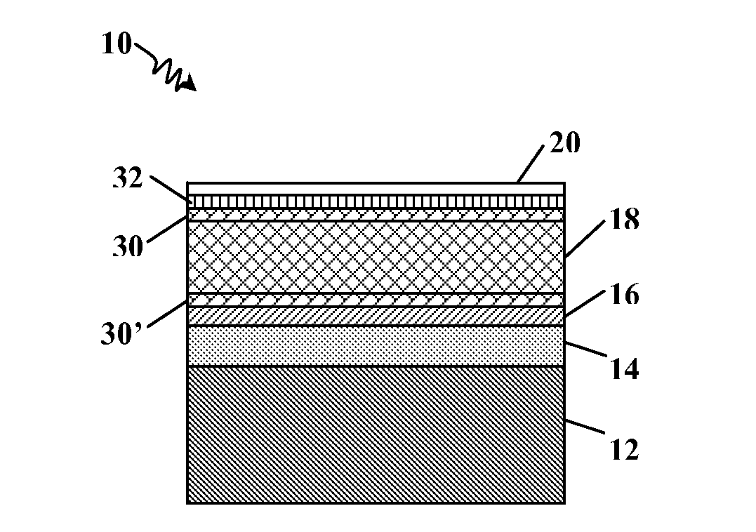
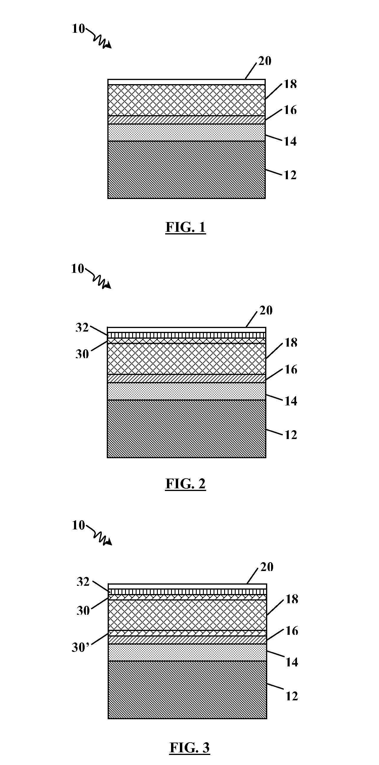
[0017]For a copper-containing contact metal on p-CdTe, the cadmium fluoride barrier layer should be of a thickness that impedes the diffusion of copper through the cell while allowing
tunneling current from the p-type cadmium telluride layer to the back contact. In one embodiment, the thickness is less than about 25 nm or less than about 10 nm. The CdF2 barrier layer facilitates the establishment of a thermally-stable low-resistance contact between the p-type cadmium telluride layer and the back contact, which increases the efficiency and lifetime of the photovoltaic cell.
[0019]In some embodiments, the forming step may create a
copper fluoride barrier layer between the diffusion impedance barrier layer and the electrical contact. In some embodiments, the diffusion impedance barrier layer impedes the diffusion of a metal from the electrical contact into the p-type layer. In other embodiments, the impedance barrier layer may have a thickness of about 0.5 to about 25 nanometers. In some embodiments, the impedance barrier layer allows the tunneling of current from the p-type layer of the photovoltaic cell to the electrical contact. Some embodiments may include the step of creating a second diffusion impedance barrier layer atop the p-type layer by exposing at least one surface of the first diffusion impedance barrier layer to a
halogen (e.g., fluorine).

