

Method for Producing Silicon Nitride Films
- Summary
- Abstract
- Description
- Claims
- Application Information
AI Technical Summary
Benefits of technology
Problems solved by technology
Method used
Image

Examples
example 1
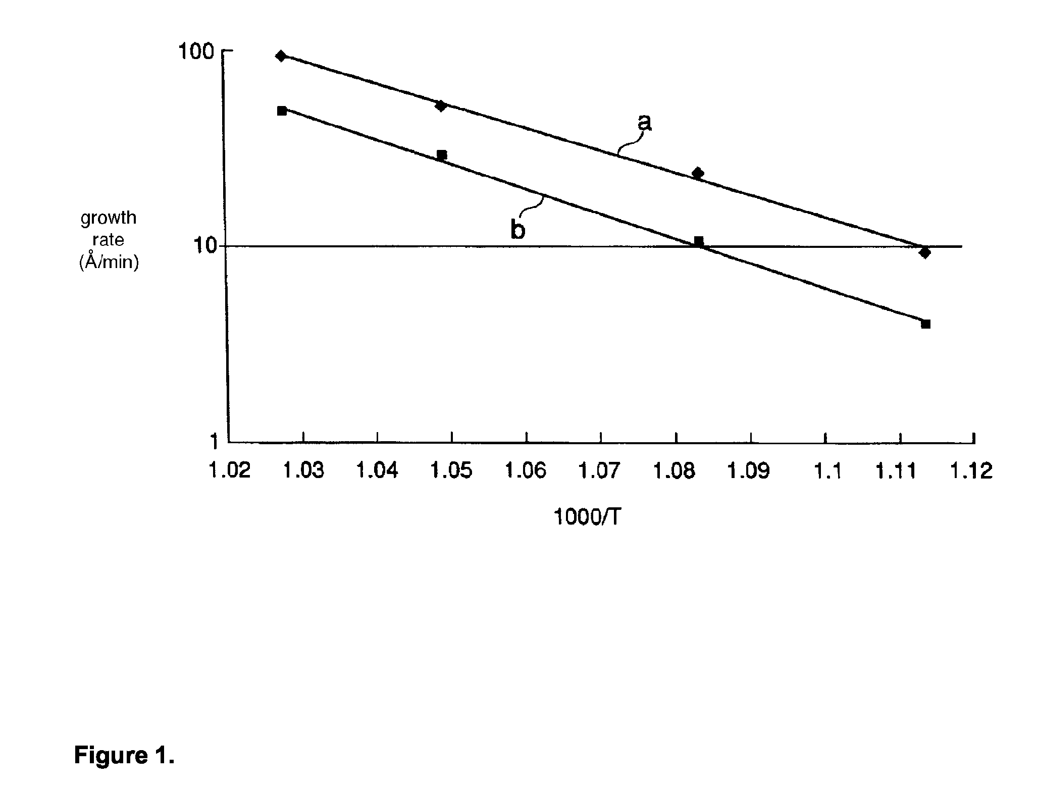
[0025]Silicon nitride film was produced at different CVD reaction temperatures (T) on silicon substrate held in a reaction chamber by delivering T SA gas into the reaction chamber at a feed flow rate of 0.5 sccm, ammonia at a feed flow rate of 40 sccm, and trimethylamine (TMA) at a feed flow rate of 40 sccm while maintaining a pressure of 1 torr in the reaction chamber. The silicon nitride deposition (growth) rate was measured during film production and was plotted against 1000× the reciprocal of the reaction temperature (T in kelvin (K)). The results are plotted as line a in FIG. 1.
example 2
[0028]Silicon nitride was grown on silicon substrate in a reaction chamber using the following CVD reaction conditions.
[0029]TSA flow rate: 0.5 sccm
ammonia flow rate: 20 sccm
TMA flow rate: 20 sccm
pressure in the reaction chamber: 100 torr
CVD reaction temperature: 500° C.
[0030]The resulting rate of silicon nitride growth was 102 Å / min. The obtained silicon nitride film was exposed to the atmosphere for 1 week, after which time the oxygen concentration in the silicon nitride film was measured by Auger electron spectroscopic analysis. It was found as a result that there was almost no oxygen in the film. In addition, the carbon concentration in the film was ≦5 atom %.
[0031]An etching rate of less than 1 Å / min was observed when the obtained silicon nitride was immersed in 1% hydrofluoric acid. The silicon nitride film obtained according to the present invention was therefore confirmed to have an excellent resistance to etching with hydrofluoric acid (refer to the results in Comparative E...
examples 3 and 4
[0032]Silicon nitride films were deposited using the same CVD reaction conditions as in Example 2, but in these examples using reaction temperatures of 490° C. and 480° C. The rate of silicon nitride film growth was 20 Å / min in the former case and was 4.4 Å / min in the latter case. This confirmed that execution of this invention can provide satisfactory silicon nitride film growth even at temperatures as low as less than 500° C.
PUM
| Property | Measurement | Unit |
|---|---|---|
| Temperature | aaaaa | aaaaa |
| Temperature | aaaaa | aaaaa |
| Pressure | aaaaa | aaaaa |
Abstract
Description
Claims
Application Information