Semiconductor memory device

a memory device and semiconductor technology, applied in the field of semiconductor memory devices, can solve the problems of increasing ac (alternating current)-wise current, affecting the performance of the memory cell capacitor, so as to achieve the effect of reducing the bandwidth of data transfer, reducing the cost of storage and storage, and increasing the data bus width

Active Publication Date: 2008-11-13
RENESAS ELECTRONICS CORP
View PDF3 Cites 87 Cited by
  • Summary
  • Abstract
  • Description
  • Claims
  • Application Information

AI Technical Summary

Benefits of technology

[0005](1) a load of a signal interconnection line is lower than that of an on-board interconnection line and data or a signal can be transmitted at high speed;
[0006](2) as the number of pin terminals is not restricted, a data bus width can be greater and a bandwidth for data transfer can be greater;
[0007](3) as each component is integrated on the single semiconductor chip, a small and compact system can be implemented; and
[0008](4) a macro prepared as library can be arranged for a component to be formed on the semiconductor chip and design efficiency can be i...

Problems solved by technology

In the DRAM, however, electric charges stored in the memory cell capacitor are lost due to various types of leakage currents such as a junction leakage current at a storage node (connection node between the memory cell capacitor and an access transistor), a channel leakage current of a memory cell transistor (access transistor), a gate leakage current of a capacitor insulating film, and the like.
Therefore, as signal lines are charged and discharged and circuitry in a portion related to row selection operates, consumption of AC (alternating current)-wise current increases.
In addition, with the increase in the storage capacity and shrinking in feature size, consumption of DC (direct current)-wise current due to an off-leakage current of the transistor in an internal ci...

Method used


Image

  • Semiconductor memory device
  • Semiconductor memory device
  • Semiconductor memory device

Examples


first embodiment

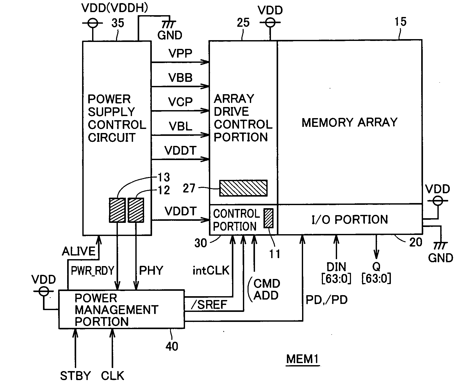
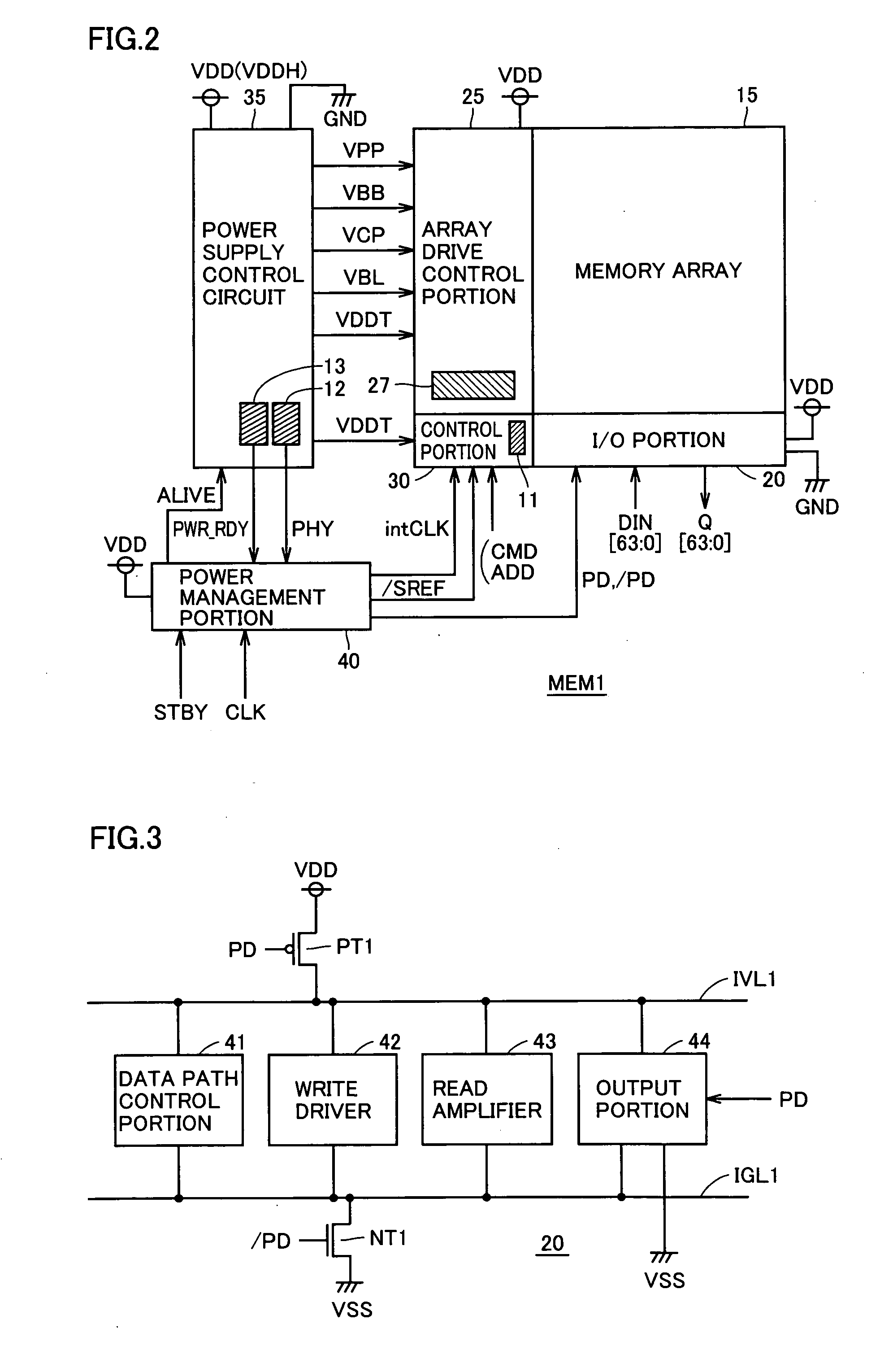
[0075]FIG. 2 schematically shows an overall configuration of memory circuit MEM1 according to the first embodiment of the present invention. In FIG. 2, memory circuit MEM1 includes a memory array 15 having a plurality of memory cells arranged in rows and columns, an I / O portion (input and output portion: data path) 20 transmitting and receiving data to and from memory array 15, and an array drive control portion 25 driving the memory cell in memory array 15 to a selected / non-selected state.

[0076]More specific configuration of memory cell array 15 and array drive control portion 25 will be described later. Here, a drive power supply control portion 27 provided in array drive control portion 25 is representatively shown. Most circuits in drive power supply control portion 27 receive a power supply voltage VDDT supplied from a power supply control circuit 35 as an operating power supply voltage, however, some circuits receive an external power supply voltage VDD to carry out control fo...

second embodiment

[0236]FIG. 21 schematically shows an overall configuration of the memory circuit (DRAM core) according to the second embodiment of the present invention. DRAM core MEM1 shown in FIG. 21 is different from DRAM core MEM1 shown in FIG. 2 in the configuration in the following points. Specifically, external high-side power supply voltage VDDH is supplied to array drive control portion 25. High-side power supply voltage VDDH is a voltage higher than the voltage level of high voltage VPP. The configuration of the memory circuit shown in FIG. 21 is otherwise the same as that of the memory circuit shown in FIG. 2. Therefore, the corresponding components have the same reference characters allotted and detailed description thereof is not provided.

[0237]FIG. 22 schematically shows a configuration of power supply to the sub block in array drive control portion 25 shown in FIG. 21. In FIG. 22, a high-side main power supply line 120 is provided in common to sub blocks MB0 to MBk. High-side main po...

third embodiment

[0257]FIG. 26 shows a configuration of high-voltage power supply control circuit 75 included in drive power supply control circuit 27 according to the third embodiment of the present invention. In high-voltage power supply control circuit 75 shown in FIG. 26, a decoupling capacitance 130 is provided for local high voltage line 67. In addition, in high-voltage power supply control circuit 75, as in the configuration of the low-side power supply control portion in the previous second embodiment, MOS transistor NQ20 for isolating the ground line and MOS transistor 127 for clamping the global negative voltage are provided. Local high voltage line 67 is coupled to the global high voltage line (66) through the high voltage node.

[0258]The configuration of the word line driver and negative voltage setting circuit 70 shown in FIG. 26 is the same as that shown in the previous first and second embodiments, and arrangement of local high voltage line 67, local ground line 77 and local negative v...


PUM


Abstract

During a stand-by state in which power supply is cut off, a high-voltage power supply control circuit isolates a global negative voltage line transmitting a negative voltage and a local negative voltage line provided corresponding to each respective sub array block from each other and isolates a global ground line and a local ground line transmitting a ground voltage from each other. These local ground line and local negative voltage line are charged to a high voltage level through a high voltage line before cut-off from the corresponding power supply. A leakage current path from a word line to the negative voltage line or the ground line is cut off, so that the word line in a non-selected state can reliably be maintained at a non-selection voltage. Thus, in a low power consumption stand-by mode, data stored in a memory cell can be held in a stable manner.

Description

BACKGROUND OF THE INVENTION[0001]1. Field of the Invention[0002]The present invention relates to a semiconductor memory device, and particularly to an embedded memory integrated on a single semiconductor chip together with a processing device such as a logic. More specifically, the present invention relates to a configuration for reducing current consumption without deteriorating data hold characteristic of a memory cell in a deep power down mode (low current consumption stand-by mode) of an embedded DRAM (dynamic random access memory).[0003]2. Description of the Background Art[0004]In the fields of image data processing and the like, in order to perform high-speed data processing, a system LSI (large scale integrated circuit) in which a logic circuit such as a processor and a memory circuit are integrated on a single semiconductor chip has widely been used. In the system LSI, as the logic circuit and the memory circuit are interconnected via on-chip interconnects, the following adv...

Claims


Application Information

Patent Timeline
IPC IPC(8): G11C7/00G11C5/14G11C8/00
CPCG11C5/063G11C5/14G11C5/148G11C11/406G11C11/4074G11C2211/4067
Inventor SHIMANO, HIROKIARIMOTO, KAZUTAMI
Owner RENESAS ELECTRONICS CORP
Why Eureka
Try Eureka