Method of making thin film transistors comprising zinc-oxide-based semiconductor materials

a technology of zinc oxide and semiconductor materials, applied in the direction of sustainable manufacturing/processing, semiconductor devices, climate sustainability, etc., can solve the problems of amorphous silicon, difficult or complicated processes, and most organic semiconductors generally have inferior or problematic electronic properties, etc., to achieve excellent field-effect electron mobility, stable threshold voltage, and sufficient performance properties

Inactive Publication Date: 2008-12-04
EASTMAN KODAK CO
View PDF8 Cites 104 Cited by
  • Summary
  • Abstract
  • Description
  • Claims
  • Application Information

AI Technical Summary

Benefits of technology

[0027]Semiconductor films made by the present method are capable of exhibiting, in the film form, stable threshold voltages and excellent field-effect electron mobility of greater than 0.01 cm2/Vs and on-off ratios of greater than 104, in which performance properties are sufficient for use in a variety of relevant technologies, including active matrix display backplanes.
[0028]One embodiment of the present invention is directed to the use of such n-channel semiconductor films in thin f

Problems solved by technology

The deposition of amorphous silicon, during the manufacture of transistors, requires relatively difficult or complicated processes such as plasma enhanced chemical vapor deposition and high temperatures (about 360° C.) to achieve the electrical characteristics sufficient for display applications.
However, most organic semiconductors generally hav

Method used


Image

  • Method of making thin film transistors comprising zinc-oxide-based semiconductor materials
  • Method of making thin film transistors comprising zinc-oxide-based semiconductor materials
  • Method of making thin film transistors comprising zinc-oxide-based semiconductor materials

Examples


example 2

[0158]In this inventive example, the semiconductor layer was applied as in Comparative Example 1 and then inkjet printed silver nanoparticles were used to make the source and drain for the transistor.

[0159]Inkjet printing experiments were performed using a system consisting of a sample platen supported by a set of X-Y translation stages, piezoelectric demand-mode printheads supported by a Z translation stage, and software to control these components. The printheads of this inkjet system are suited to dispense droplets in the 20-60 picoliter range. Approximately 2 cc of the fluid to be printed is placed in a sample cartridge which is then screwed to the printing fixture. The printhead is primed with ink using pressurized nitrogen. A TENCOR profilometer was used to measure the printed film thicknesses of a series of calibration samples. The drop volume was calculated by best-fit linear regression in a simple model relating number of drops fired, ink concentration, and printed film thi...

example 3

[0164]This Example shows a variety of inkjet printed silver contact electrodes applied to a variety of inkjet-printed ZnO semiconductor films in thin film transistors made according to the present invention. In these examples, the ZnO semiconductor films were printed using the same inkjet printer as used for the making the source and drain from the silver nanoparticles.

[0165]The variety of inkjet-printed ZnO-semiconductor films were prepared as follows. A 30 mm square sample of a silicon wafer was cleaned according to the procedure described above and placed on the printhead stage. A 3.31 wt % dispersion of charge stabilized ZnO nanoparticles was diluted with ethanol to 1.3 wt %, and an ink cartridge was filled with the resulting fluid. By overlaying drops at different drop spacing, a set of ZnO nanoparticle films with varying film thickness were obtained. The samples were heated for 10 minutes at 200° C. in air. A 0.175 molar zinc acetate solution in methanol was then printed on to...

example 5

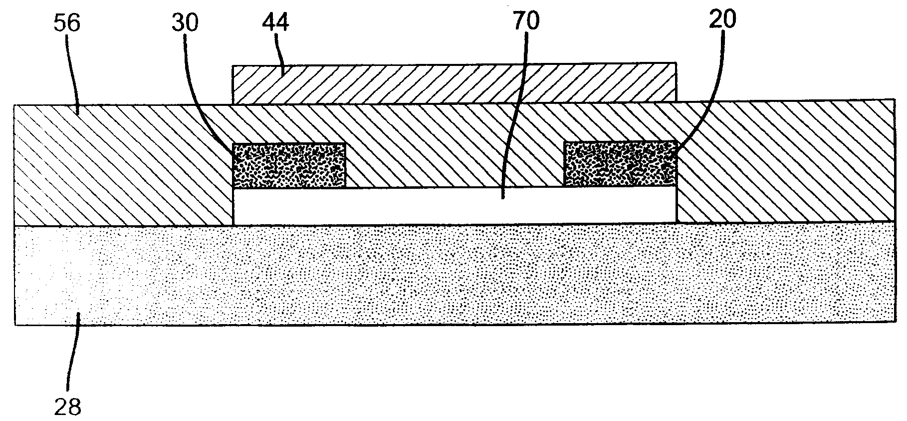
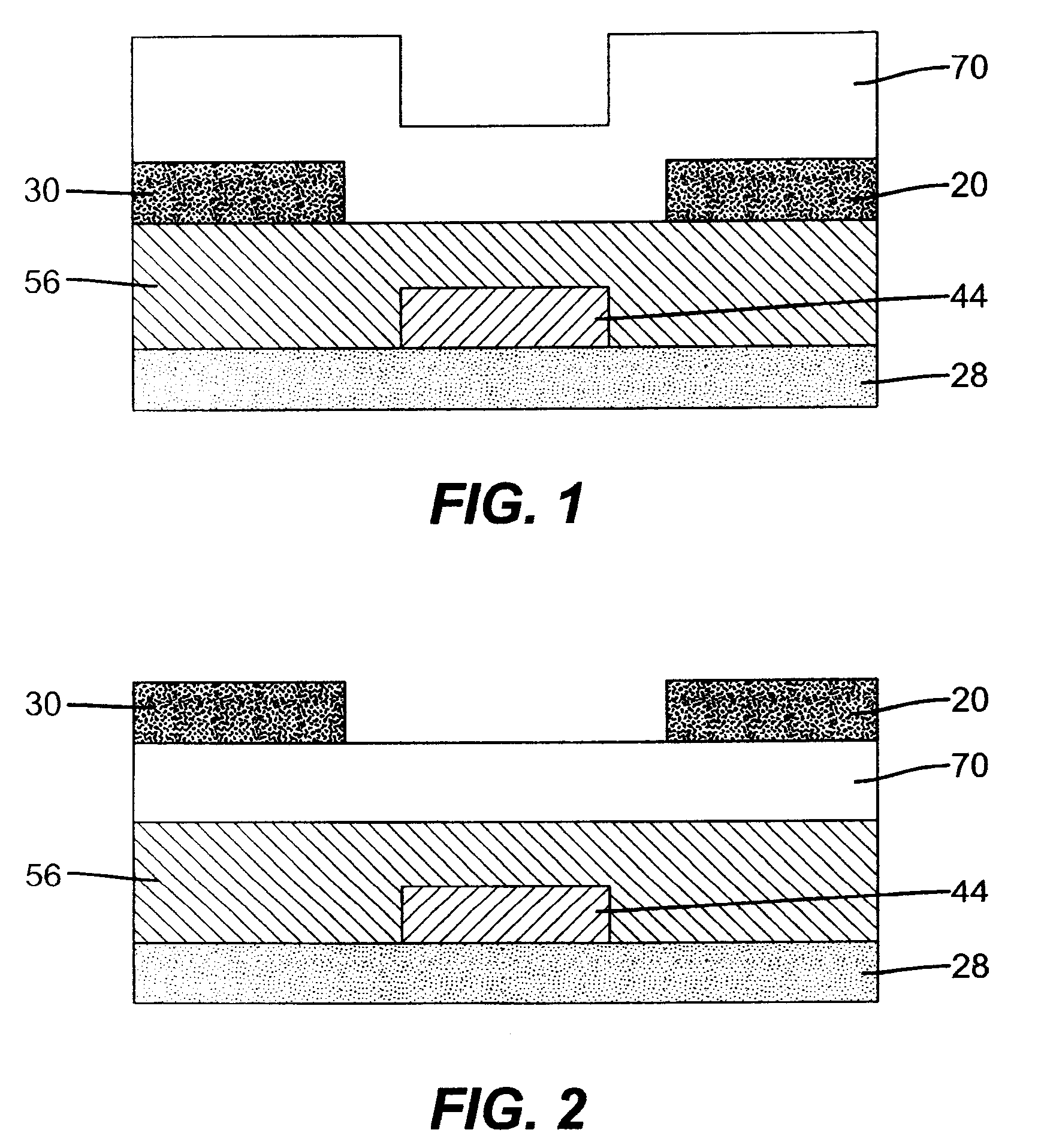
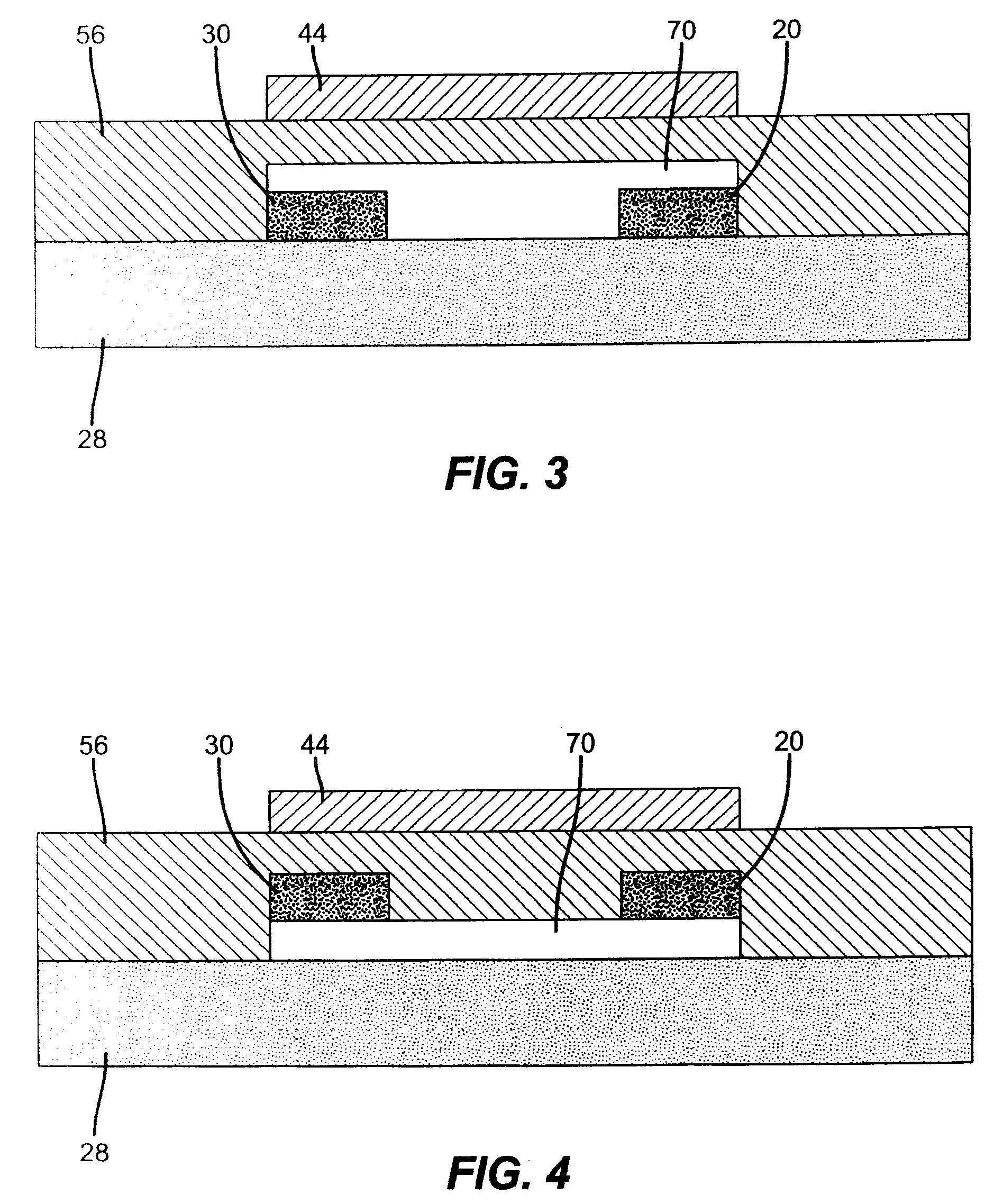
[0173]In this example, TFT structures were prepared in the same manner as for Comparative Example 4, except inkjet printed silver nanoparticles were employed in making the source and drain. After deposition of the zinc oxide film, a photoresist pattern was prepared on the ZnO coating containing pairs of open rectangular areas, which defined the desired shape and arrangement of the source and drain regions of the TFTs. The ZnO coating between a specific pair of open rectangular areas was therefore covered by the photoresist material, which defined the shape and location of the channel of that particular TFT. Using the inkjet printing system described in Example 2, the substrate was placed on the sample holder at 60° C., and a top-view camera was used to locate the open rectangular areas on the ZnO coating. A commercially available silver dispersion purchased from Cabot (Albuquerque, N. Mex.), was diluted 1:1 with water and deposited specifically onto the open rectangular areas on the...


PUM


Abstract

A method of making a thin film transistor comprising a zinc-oxide-containing semiconductor material and spaced apart first and second electrodes in contact with the material. The co-generation of high quality zinc oxide semiconductor films and contact electrodes is obtained, at low temperatures, using non-vacuum conditions, silver nanoparticles are deposited to form the source and drain and, upon heating, converted to conducting metal. Such an in-situ formation of the silver metal/zinc oxide interface provides superior transistor activity compared to evaporated silver.

Description

FIELD OF THE INVENTION[0001]The present invention relates to a method of making thin film transistors in which a colloidal solution of silver nanoparticles is printed onto a zinc-oxide-based semiconductor film. Such thin film transistors can be used in electronic devices, particularly in displays in which low temperature processes of making the thin film transistors are advantageous.BACKGROUND OF THE INVENTION[0002]For applications in which a transistor needs to be applied to a substrate, a thin film transistor is typically used. Thin film transistors (TFTs) are widely used as switching elements in electronics, for example, in active-matrix liquid-crystal displays, smart cards, and a variety of other electronic devices and components thereof. The thin film transistor (TFT) is an example of a field effect transistor (FET). The best-known example of an FET is the MOSFET (Metal-Oxide-Semiconductor-FET), today's conventional switching element for high-speed applications. A critical step...

Claims


Application Information

Patent Timeline
IPC IPC(8): H01L29/22H01L21/34
CPCH01L21/02554H01L21/02565H01L21/02628H01L27/1225H01L29/7869Y02P70/50
Inventor IRVING, LYN M.LEVY, DAVID H.CHILDS, ANDREA C.
Owner EASTMAN KODAK CO
Why Eureka
Try Eureka