Thin Film Semi-Conductor-on-Glass Solar Cell Devices

a technology of thin film semiconductor and semi-conductor, applied in the field of solar cells and thin film transistors, can solve the problems of inefficient utilization of solar spectrum, limited thermal budget required, and high manufacturing cost, and achieve the effect of inhibiting transport and deleterious action, degrading the electronic and/or optical performance of the said devi

Inactive Publication Date: 2008-12-18
IQE
View PDF3 Cites 68 Cited by
  • Summary
  • Abstract
  • Description
  • Claims
  • Application Information

AI Technical Summary

Benefits of technology

[0013]The present invention relates to semiconductor devices combined with an inexpensive substrate for electronic and optoelectronic applications. In a particular form the present invention relates to fabrication of a solar cell and / or thin film transistor (TFT) through the combination of rare-earth metal, rare-earth metal-oxides-nitrides, -phosphides and -carbides and Group IV, III-V, and II-VI semiconductors and alloys disposed upon inexpensive substrates, such as glass. In an embodiment, thin film semiconductor materials composed of silicon (Si) and / or germanium (Ge) are disposed upon cost effective silicon dioxide (SiO2) based glass substrate. Such semiconductor-on-glass (SoG) articles are applicable to thin film transistor and solar cell manufacture. The present invention discloses the use of a functional barrier layer disposed between a thin film semiconductor layer and an inexpensive substrate so as to inhibit transport and deleterious action of impurity species migrating from the substrate into a thin film semiconductor, thereby degrading the electronic and / or optical performance of the said device. Optionally, a functional barrier layer may serve as an alternative barrier between an inexpensive substrate and a functional device disposed thereon; examples of types of barriers are thermal, mechanical, chemical, optical, and / or other radiation deleterious to a functional device and / or from a device to its substrate.
[0015]Thin film semiconductor-on-glass application to solar cell and TFT devices benefit from the insulating nature of the glass substrate and can be designed as ideal thin film semiconductor-on-insulator (SOI) structures. For mass manufacture of SoG the utility of a glass substrate is primarily due to the potential low cost of alkali-silicate glasses. However, it has long been known by workers in the field of glass manufacture that most compositions of alkali-silicate glasses exhibit some electrical conductivity. The electrical activity of the alkaline-silicate glasses is directly attributable to mobile positive alkaline ions through the silicate network; in addition inexpensive glasses may contain high levels of boron, lead and other elements injurious to a semiconductor. Optional inexpensive substrates contain alternative elements not acceptable to a solid-state device; in general some type of barrier must isolate a semiconductor device from some property of an inexpensive substrate.
[0016]It is an object of one embodiment of the present invention to fully utilize the low cost of alkaline-silicate glasses for use in SoG and increase the performance of devices formed by use of alkaline barrier layers. An example embodiment, but not limited to, is the use of rare-earth compound(s), such as a rare-earth oxide (REOx), comprising charged oxygen vacancies (Ovn) capable of neutralizing the migration of deleterious positive alkaline ions, such as Na+ and / or K+, into a semiconductor active region; charged oxygen vacancies (Ovn) functionally impede migration of positive ions to the extent that an active region above a barrier layer functions within specification.
[0017]For certain applications, poly-Si thin film transistors and / or optoelectronic devices provide an acceptable trade-off between performance and cost. For large volume applications such as flat panel displays and solar cells, it is also desirable to further reduce the cost of manufacture of thin films on glass and increase crystalline structure perfection to that approaching high quality single crystal. Furthermore, it is advantageous to develop a process of SoG manufacture requiring low thermal budget.

Problems solved by technology

Unfortunately, prior art techniques for producing sc-Si cells are: (i) costly to manufacture; and (ii) suffer inefficient utilization of the available solar spectrum.
Typically, the use of low cost substrates places limitation upon thin film semiconductor crystal quality and / or thermal budget required for thin film deposition method of a thin film(s).
Low thermal budget deposition of thin films typically results in poor crystal quality semiconductors realized upon amorphous glass substrates.
Single semiconductor crystals may nucleate in localized areas upon an initial glass substrate surface, but formation of homogeneous and long range crystal order within the thin film across substantially the entire large area glass substrate is practically impossible without complex post growth recrystallization.
Even so, the film quality attained using prior art complex recrystallization techniques is still inferior to bulk single crystal growth techniques, such as, the Czochralski crystal growth (CZ) method.
Furthermore, the growing film must adequately wet the substrate surface for layer-by-layer epitaxy, otherwise clustered nucleation growth occurs and thus structurally defective.
It is well known that large area single crystal thin film semiconductors cannot be directly deposited epitaxially upon glass and / or amorphous substrates.
The design compromise for the structural quality of the thin film is therefore between cost and whether single-crystal or polycrystal thin films are required for a specific application.
Prior art techniques to date fail to address the implication of the intrinsic chemical property of cheap substrate composition; for instance, glass is typically alkali-silicate-based and quite severely impacts the electronic and / or optoelectronic performance of a thin film semiconductor.
It is therefore not well known by researchers in the field of thin film semiconductor manufacture, the fact that it is not a simple matter of replacing the substrate with a cheap alternative, such SiO2-based glass, because of the typically chemically disruptive influence on at least one of the thin film electronic and / or optical and / or chemical and / or mechanical properties.
For an example case of using cheap SiO2-based glass substrate to form SoG article, regardless of the thin film semiconductor manufacture technique (i.e.; via layer-transfer or direct deposition), the chemical composition of cheap glass poses severe contamination concerns for electronic and optoelectronic performance of thin film devices.

Method used


Image

  • Thin Film Semi-Conductor-on-Glass Solar Cell Devices
  • Thin Film Semi-Conductor-on-Glass Solar Cell Devices
  • Thin Film Semi-Conductor-on-Glass Solar Cell Devices

Examples


example i

Metal-Insulator-Semiconductor Solar Cell Using SoG

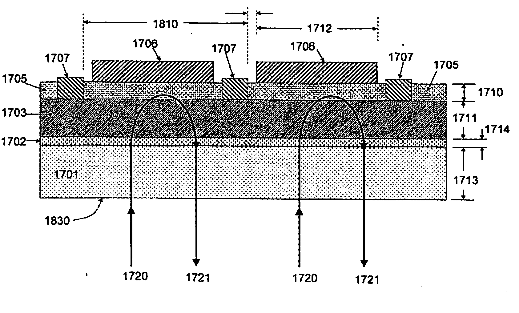
[0121]A metal-insulator-semiconductor (MIS) device fabricated upon a glass substrate is disclosed in FIGS. 17A & 17B. The thin film single crystal semiconductor layer 1703 is fabricated upon a transparent substrate 1701 according to the methods of the present invention. Layer 1703 with thickness 1711 is chosen from single crystal Si, and the substrate 1701 with thickness 1713 is chosen from low cost alkali-silicate glass. An alkali barrier layer 1702 with thickness 1714 separates the thin film semiconductor 1703 from the glass substrate 1701 in order to prevent alkali ion contamination.

[0122]The SoG substrate is fabricated into the MIS device via optional selective oxidation of thin film Si layer 1703 into SiO2 regions 1704 and / or 1705. Layer 1705 is a dielectric and / or insulating material and can be chosen from SiO2, SiNx or single crystal rare-earth oxide compositions as disclosed in patent # U.S. Pat. No. 7,199,015, titled “Rare-e...

example ii

P-I-N Solar Cell Using SOG

[0126]Another embodiment of the present invention is the use of multilayer semiconductor structures disposed upon the glass substrate. Another embodiment is the use of single crystal semiconductor layers to form the active regions. Yet another embodiment is the use of Si layers chosen from not-intentionally doped (i.e., substantially intrinsic, i), n-type (n) and p-type (p) doping. For solar energy conversion devices, layered Si devices of the form of p-n and p-i-n diodes are efficient optoelectronic conversion structures. An example p-i-n SoG embodiment is shown in FIG. 19A. The fabrication of the p-i-n SoG structure is possible using the methods disclosed in the present invention. It is understood that p-n junctions and more complex structures are also possible. The glass substrate 1701 is separated from the single crystal thin film semiconductor 1902 layer via a barrier layer 1702 according to the methods disclosed.

[0127]The p-i-n layer structure is comp...

example iii

Multi-junction Wavelength Dependent Absorber Section Solar Cell Using SoG

[0130]The absorption co-efficient as function of wavelength for the thin film semiconductor layer can be used for selecting the thickness and wavelength region operation. In particular, Si exhibits a highly non-linear absorption character as a function of optical wavelengths. Referring to FIG. 16A, it can be seen πabs(λ) in Si varies by almost five orders of magnitude in the range 350≦λ≦1127 nm. Short wavelength photons are therefore absorbed in a very short distance compared to long wavelength photons in the vicinity of the indirect band gap EG.

[0131]Silicon Tandem Cell Based on Selective Absorption

[0132]FIG. 22A discloses a stacked layer structure consisting of two p-i-n diodes comprising different intrinsic absorber thicknesses. In preference, the semiconductor is selected from single crystal Si and the substrate from alkaline-silicate glass. An example embodiment discloses a first p-i-n diode comprising p:S...


PUM

PropertyMeasurementUnit
transparentaaaaaaaaaa
band gapaaaaaaaaaa
radiation of wavelengthaaaaaaaaaa

Abstract

The present invention relates to semiconductor devices suitable for electronic, optoelectronic and energy conversion applications. In a particular form, the present invention relates to the fabrication of a thin film solar cells and thin film transistors through the advantageous combination of semiconductors, insulators, rare-earth based compounds and amorphous and / or ceramic and / or glass substrates. Crystalline or polycrystalline thin film semiconductor-on-glass formation using alkali ion impurity barrier layer(s) are disclosed. Example embodiment of crystalline or polycrystalline thin film semiconductor-on-glass formation using rare-earth based material as impurity barrier layer(s) is disclosed. In particular, thin film silicon-on-glass substrate is disclosed as the alternate embodiment, with impurity barrier designed to inhibit transport of deleterious alkali species from the glass into the semiconductor thin film.

Description

PRIORITY[0001]This application claims priority from Provisional application 60 / 944,369 filed on Jun. 15, 2007.CROSS REFERENCE TO RELATED APPLICATIONS[0002]Applications and patents 09 / 924,392, 10 / 666,897, 10 / 746,957, 10 / 799,549, 10 / 825,912, 10 / 825,974, 11 / 022,078, 11 / 025,363, 11 / 025,680, 11 / 025,681, 11 / 025,692, 11 / 025,693, 11 / 084,486, 11 / 121,737, 11 / 187,213, U.S. 20050166834, U.S. 20050161773, U.S. 20050163692, 11 / 053,775, 11 / 053,785, 11 / 054,573, 11 / 054,579, 11 / 054,627, 11 / 068,222, 11 / 188,081, 11 / 253,525, 11 / 254,031, 11 / 257,517, 11 / 257,597, 11 / 393,629, 11 / 398,910, 11 / 472,087, 11 / 788,153, 11 / 960,418, 60 / 820,438, 60 / 811,311, 60 / 847,767, 60 / 905,419, 60 / 905,945, 60 / 944,369, 60 / 949,753, U.S. Pat. No. 7,018,484, U.S. Pat. No. 7,037,806, U.S. Pat. No. 7,135,699, U.S. Pat. No. 7,199,015, all held by the same assignee, contain information relevant to the instant invention and are included herein in their entirety by reference. References, noted at the end, are included herein in their entiret...

Claims


Application Information

Patent Timeline
Patent Type & Authority Applications(United States)
IPC IPC(8): H01L31/00H01L21/762
CPCC03C17/36C03C17/3636C03C17/3642C03C17/3678H01L31/03921H01L31/1055Y02E10/50
Inventor ATANACKOVIC, PETAR
Owner IQE
Why Eureka
Try Eureka