Semiconductor device and manufacturing method thereof

a semiconductor and manufacturing method technology, applied in semiconductor devices, instruments, optics, etc., can solve the problems of difficult to employ the above-described process for a display device, and achieve the effect of improving mobility, extremely easy to achieve, and improving mobility

Inactive Publication Date: 2009-01-01
SEMICON ENERGY LAB CO LTD
View PDF12 Cites 4 Cited by
  • Summary
  • Abstract
  • Description
  • Claims
  • Application Information

AI Technical Summary

Benefits of technology

[0023]Further, the step of applying compressive strain to the semiconductor layer is a step utilizing part of shrink by heat treatment of the substrate, which has been performed conventionally, without adding any new step, and can be realized extremely easily, which is a great advantage.
[0024]Therefore, when a transistor in which an effect of improvement in mobility can be obtained by using compressive strain and a transistor in which an effect of improvement in mobility can be obtained by using tensile strain are used, a semiconductor device which can perform operations more efficiently at high speed is provided.

Problems solved by technology

However, since a semiconductor layer having favorable crystallinity cannot be obtained when such a step is performed at a process temperature equal to or lower than a strain point of glass or the like, it has been difficult to employ the above-described process for a display device or the like in which a substrate needs light-transmitting properties.

Method used


Image

  • Semiconductor device and manufacturing method thereof
  • Semiconductor device and manufacturing method thereof
  • Semiconductor device and manufacturing method thereof

Examples


embodiment mode 1

[0037]A method for manufacturing a semiconductor device of the present invention is described with reference to FIGS. 1A to 6C.

[0038]A method for providing a single-crystal semiconductor layer over a substrate having an insulating surface is described with reference to FIGS. 2A to 2E and FIGS. 3A to 3D.

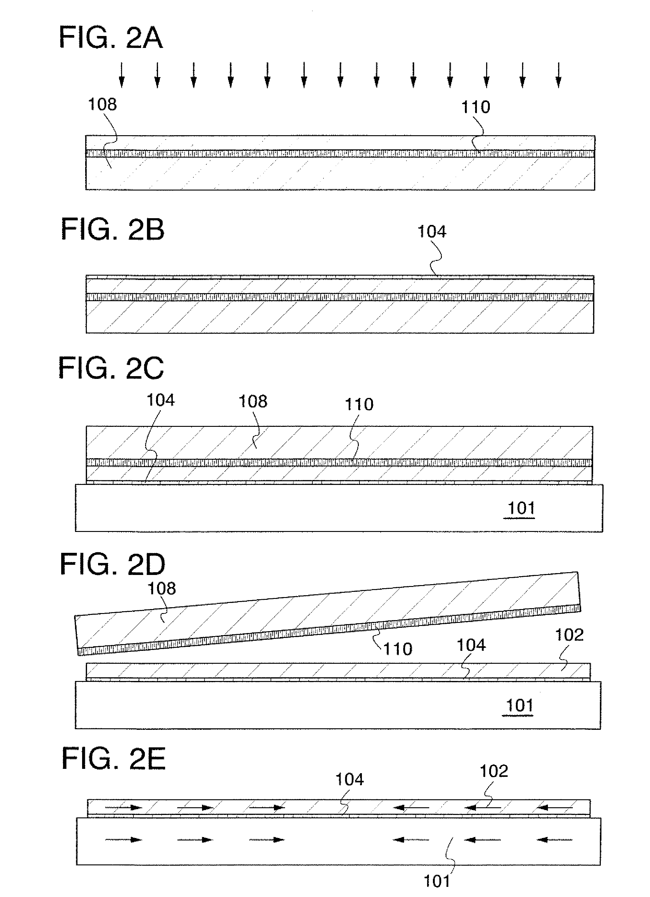
[0039]A semiconductor substrate 108 shown in FIG. 2A is cleaned, and ions which are accelerated by an electric field are introduced into the semiconductor substrate 108 from the surface thereof to reach a predetermined depth to form a weakened layer (a separation layer) 110. Ion irradiation is performed in consideration of the thickness of a single-crystal semiconductor layer which is formed over a base substrate. The thickness of the single-crystal semiconductor layer is preferably equal to or greater than 1 μm and equal to or less than 3 μm. Accelerating voltage for irradiating the semiconductor substrate 108 with ions is set in consideration of such a thickness.

[0040]A p-type or n-...

embodiment mode 2

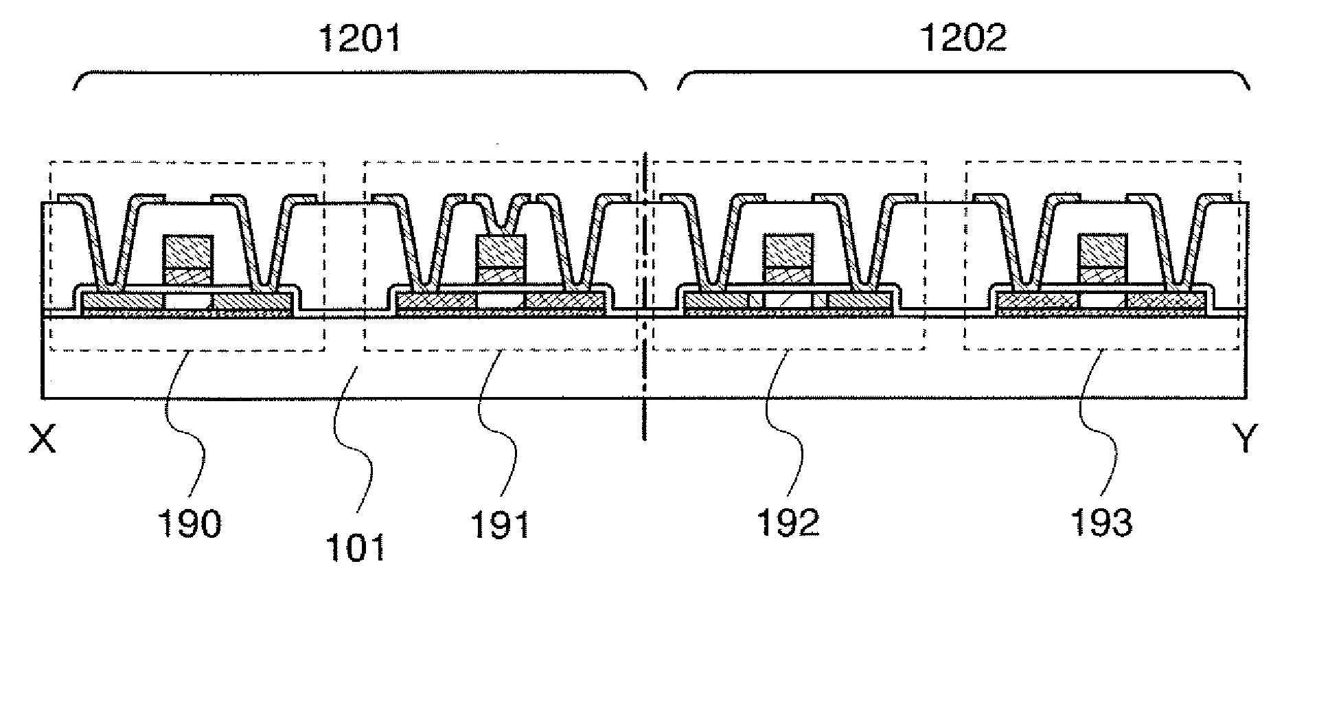
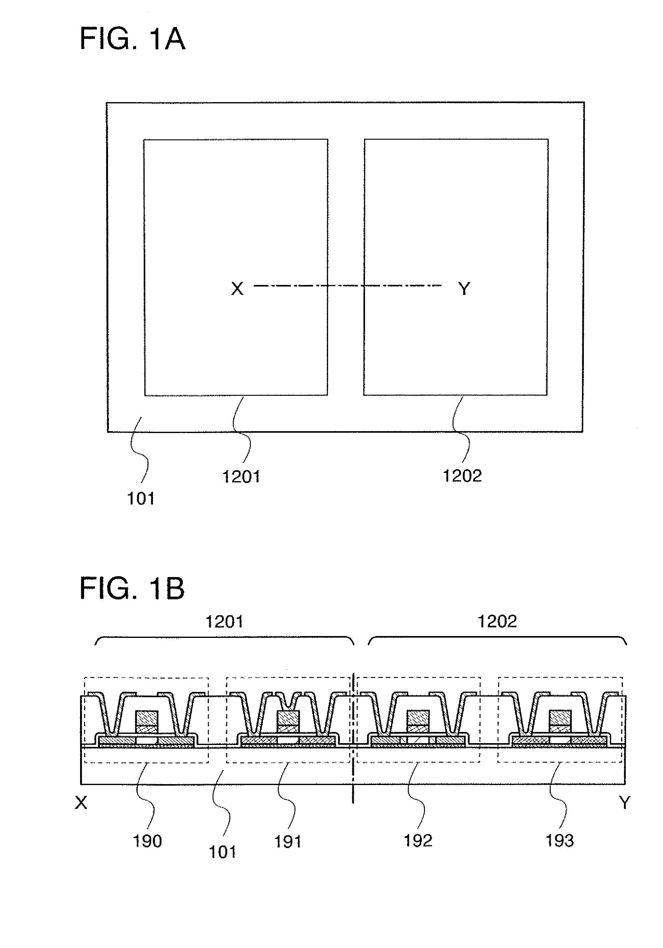
[0107]In this embodiment mode, an example of a semiconductor device having a display function, to which the present invention is applied, is described with reference to FIGS. 7A and 7B.

[0108]FIG. 7A shows an active matrix display device. A pixel portion 1002 where a plurality of pixel circuits are arranged in matrix, a data driver 1003, and a scan driver 1004 are formed over a base substrate 1001. Further, a top surface of the base substrate 1001 is hermetically sealed with a counter substrate (a sealing substrate) 1005. A control signal, an image signal, and driving power which are necessary for driving a display device are supplied from outside through a flexible printed circuit (FPC) 1006. In addition, FIG. 7B is a cross-sectional view taken along A-B in FIG. 7A.

[0109]FIG. 7B shows a cross section of an active matrix display device when a pixel portion is formed using an electroluminescence (EL) element.

[0110]The data driver 1003 and the scan driver 1004 each perform processing f...

embodiment mode 3

[0134]In the semiconductor device of the present invention, a thin single-crystal semiconductor layer 150 and a thick single-crystal semiconductor layer 160 are formed over the base substrate 101 by being attached thereto; however, there is the case where part of a separation plane due to an ion irradiation step is left remaining on an outermost surface of each single-crystal semiconductor layer. Since the separation plane is a region which is in contact with a region where the weakened layer (the separation layer) is formed by hydrogen ion irradiation, the separation plane has flatness inferior to the surface of a normal single-crystal semiconductor layer. Therefore, it is necessary to improve the surface condition of the separation plane in order to prevent defects in subsequent steps.

[0135]As a typical method for removing such a separation plane, there is surface polishing by chemical mechanical polishing (CMP) as well as a method in which the separation plane is oxidized by surf...


PUM

PropertyMeasurementUnit
thicknessaaaaaaaaaa
thicknessaaaaaaaaaa
thicknessaaaaaaaaaa

Abstract

To provide a structure and a manufacturing method for efficiently forming a transistor to which tensile strain is preferably applied and a transistor to which compressive strain is preferably applied over the same substrate when stress is applied to a semiconductor layer in order to improve mobility of the transistors in a semiconductor device. Plural kinds of transistors which are separated from a single-crystal semiconductor substrate and include single-crystal semiconductor layers bonded to a substrate having an insulating surface with a bonding layer interposed therebetween are provided over the same substrate. One of the transistors uses a single-crystal semiconductor layer as an active layer, to which tensile strain is applied. The other transistors use single-crystal semiconductor layers as active layers, to which compressive strain using part of heat shrink generated by heat treatment of the base substrate after bonding is applied.

Description

BACKGROUND OF THE INVENTION[0001]1. Field of the Invention[0002]The present invention relates to a semiconductor device including a thin film transistor over an insulating surface and a manufacturing method thereof.[0003]2. Description of the Related Art[0004]An integrated circuit has been developed, which uses a semiconductor substrate called a silicon-on-insulator (hereinafter also referred to as SOI) which has a thin single-crystal semiconductor layer over an insulating surface, instead of a silicon wafer which is manufactured by thinly slicing an ingot of a single-crystal semiconductor. An integrated circuit using an SOI substrate has attracted attention as a circuit which reduces parasitic capacitance between source and drain regions of the transistor and the substrate, and improves performance of the integrated circuit.[0005]As a method for manufacturing an SOI substrate, a hydrogen ion implantation separation method is known (e.g., see Reference 1: Japanese Published Patent A...

Claims


Application Information

Patent Timeline
Patent Type & Authority Applications(United States)
IPC IPC(8): G02F1/136H01L27/12H01L21/762
CPCH01L27/1214H01L29/78687H01L27/1266H01L21/76254H01L29/7847H01L29/7849H01L27/1262H01L27/12H01L29/7842
Inventor TANADA, YOSHIFUMI
Owner SEMICON ENERGY LAB CO LTD
Why Eureka
Try Eureka