

Carbon nanostructures and methods of making and using the same
a carbon nanostructure and nanostructure technology, applied in the manufacture of electrode systems, natural mineral layered products, electric discharge tubes/lamps, etc., can solve the problems of graphite plates that cannot be oriented on a surface, less than ideal for research studies and practical applications
- Summary
- Abstract
- Description
- Claims
- Application Information
AI Technical Summary
Benefits of technology
Problems solved by technology
Method used
Image

Examples
example 1
Preparing Substrates Using Nanosphere Lithography
[0087]Highly doped single-crystal Si (100) wafers, with a layer of 365 nm SiO2 (Silicon Materials Inc.), were used as a substrate for carbon nanoflake deposition. Commercially available, 419 nm diameter, self-assembled polystyrene nanospheres (8% Interfacial Dynamics Corporation) were used as lithography masks for preparation of periodic Ni catalysts dots. The nanospheres were received from the manufacturer as a suspension in water and then further diluted in a solution of the surfactant Triton X-100 / methanol (1:400 by volume) by a factor of 1:5. Self-assembled nanosphere single-layer masks were created by a spin-coater (Chemat Technology KW4A) at 900 rpm. Double-layer masks were obtained with lower reproducibility by increasing the nanosphere concentration in the spin-coating solution. Thin films of Ni, 10-30 nm in thickness, were then deposited on the coated Si substrates by electron-beam evaporation. After Ni deposition, the nanosp...
example 2
Forming CNF Using a Ni Catalyst on a Si Substrate
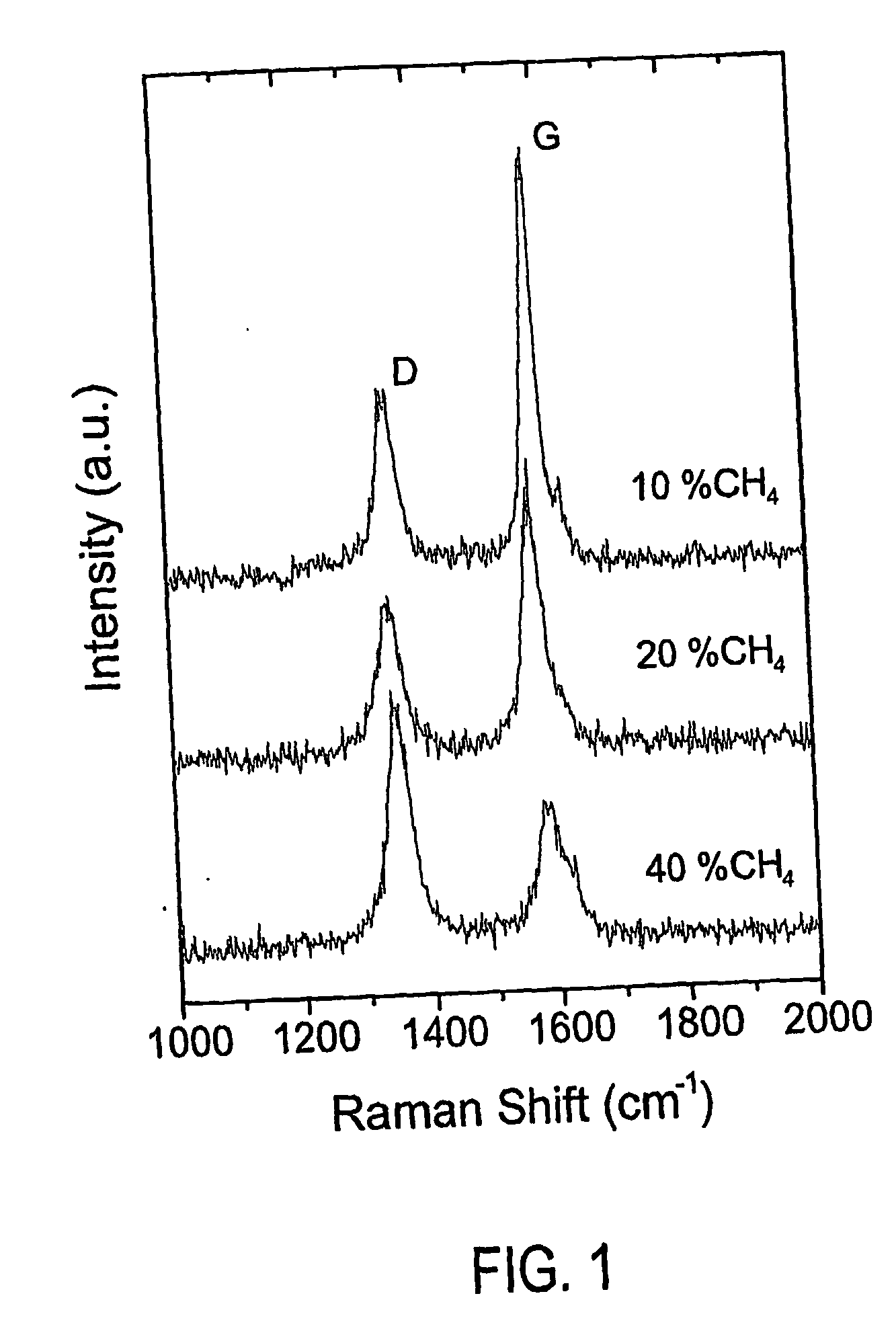
[0089]Carbon nanoflakes were grown on the substrates described in Example 1 in an inductively coupled RF-PECVD system, schematically illustrated in FIG. 24, which is very similar to FIG. 12 described above. The planar coiled RF antenna sits on the quartz window above the deposition chamber. This inductive mode RF plasma has a much higher plasma density (about 10 times) than that of capacitive systems, and also requires a lower pressure (−7 Torr provided by a 450 L / s turbo pump. During deposition, the RF power, substrate temperature, and deposition pressure were maintained at 900 W, 680° C., and 70-90 mTorr, respectively. Methane was used as the carbon source in an H2 atmosphere with the concentration of methane varying from 10% to 40%, overall gas flow rates at 10 sccm, and depositions of 5-10 min for desired sample thicknesses.
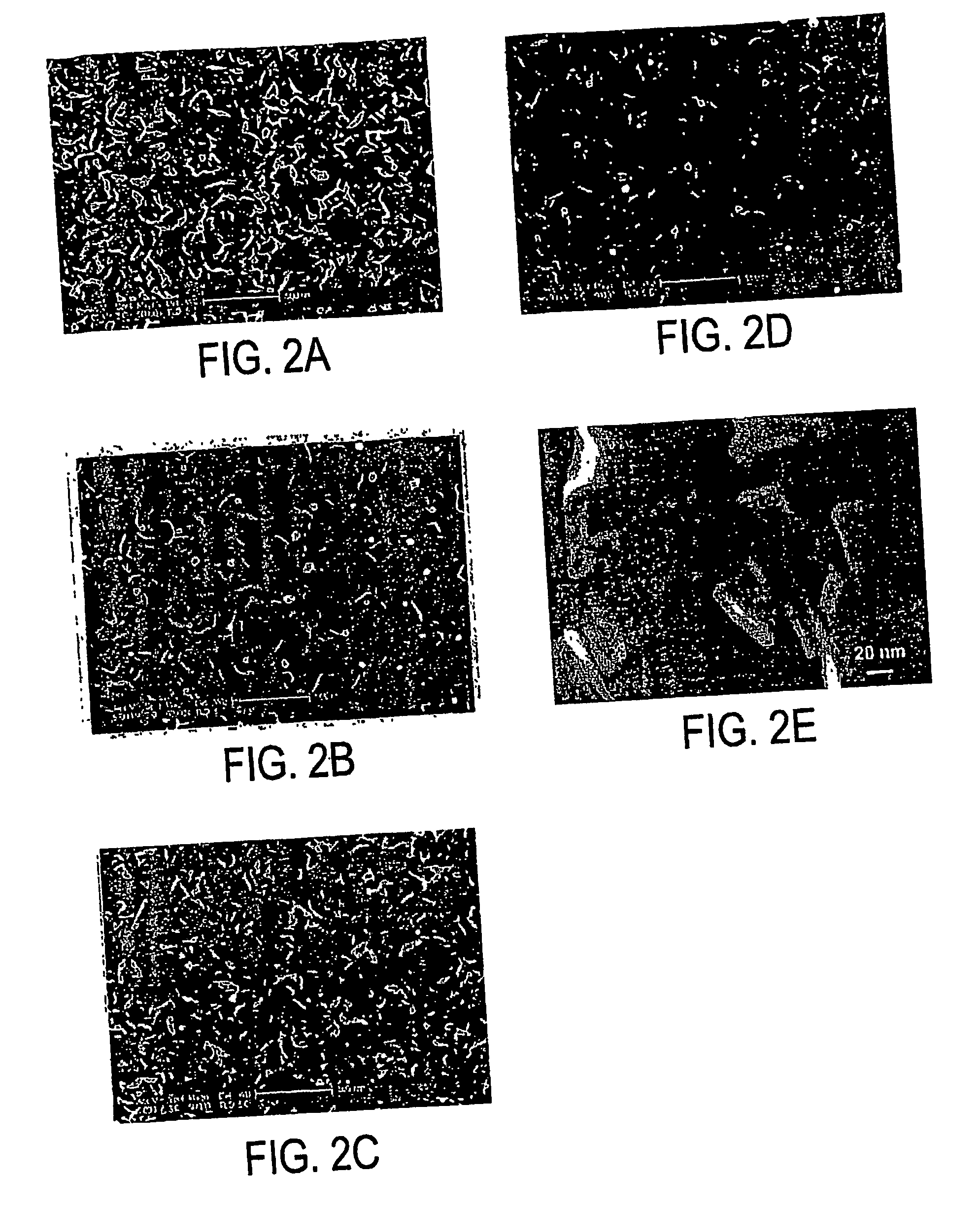
[0090]FIG. 2 shows SEM images of the resulting CNF. FIG. 1 shows the Raman spectra (Raman spectrometer—Raman...
example 3
Determining the Specific Surface Area of CNS
[0092]In order to quantify the high surface-to-volume ratio and corresponding large specific area that the atomic-scale thickness of carbon nanosheets provides, Brunauer-Emmett-Teller (BET) measurements were obtained from Clear Science Inc. (www.clearsci.com). The samples were purged with ultra high purity (UHP) nitrogen overnight at 300° C. before measurement. BET data was collected with UHP nitrogen over a pressure range from 0.05 to 0.30 relative pressure. A Micromeritics Gemini 2375 was used for the specific surface area analysis. The substrates were weighed to a standard deviation of ±0.02 mg before and after deposition using an Ohaus AP250D electronic balance. BET measurements of carbon nanosheet samples yielded a specific surface area of 1300±300 m2 / g (the large standard deviation of the electronic balance used lead to the large error in the specific surface area). This is almost the same as the theoretical value for an ideal double...
PUM
| Property | Measurement | Unit |
|---|---|---|
| Temperature | aaaaa | aaaaa |
| Temperature | aaaaa | aaaaa |
| Thickness | aaaaa | aaaaa |
Abstract
Description
Claims
Application Information