Fabrication method for carbon fiber, carbon fiber electron source, and field emission display device

a carbon fiber and electron source technology, applied in the manufacture of electrode systems, electric discharge tubes/lamps, discharge tubes luminescnet screens, etc., can solve the problems of carbon fiber abnormal growth, cramming into one dot limit, and inability to lift off the resist after catalyst sputtering, etc., to reduce abnormal growth, reduce the effect of abnormal growth and simple process

Inactive Publication Date: 2009-02-26
ROHM CO LTD
View PDF2 Cites 9 Cited by
  • Summary
  • Abstract
  • Description
  • Claims
  • Application Information

AI Technical Summary

Benefits of technology

[0029]Moreover, according to the fabrication method for carbon fiber of the present invention, since the insulating film is formed on the surface of the gate electrode, when carbon fiber grows up equal to or more than an arbitrary length and contacts a gate electrode, it is hard to become electrically short.
[0030]Moreover, according to the fabrication method for carbon fiber of the present invention, when reducing the abnormal growth, since it does not need to cover the electrode with the insulating film of SiO2 etc., the process becomes simple.
[0031]Moreover, according to the fabrication method for carbon fiber according to the present invention, it becomes possible to shorten or to control thickness for the carbon fiber grown-up too much for long, by oxidizing again.
[0032]According to the fabrication method for carbon fiber of the present invention, the abnormal growth from wiring metal electrode is prevented by a simple and cheap method by using ultrasonic selectively catalyst plating method using a field emission matrix electrode, and the carbon nano-tube of nano order based on a catalyst crystallite nucleus of nano order can be formed with high density and uniform.
[0033]Furthermore, according to the carbon fiber electron source of the present invention, the carbon fiber can be applied fabricated by the above-mentioned fabrication method for carbon fiber, and high-output current density can be achieved.
[0034]Furthermore, according to the FED device of the present invention, the carbon fiber can be applied fabricated by the above-mentioned fabrication method for carbon fiber, and high-intensity with high current density, large capacity, and a big screen can be achieved.

Problems solved by technology

However, there is a problem that the lift off of the resist after catalyst sputtering cannot be carried out since the resist denatures in a dry hole formation process accompanying miniaturization of a hole diameter.
Although there is no denaturalization of resist in wet hole formation, the hole etching is performed isotropic, and therefore cramming into one dot has a limit.
Moreover, even if a minute vertical hole is formed, there is a problem that an aspect ratio of a hole becomes large, catalyst adhesion in a hole internal wall is made at the time of catalyst sputtering, and then abnormal growth of a carbon fiber from a wall surface occurs in a growing process.
As a result, there is a problem that electron emission from each of the every matrix electrode cannot be performed.
Although a covering process of metal electrode line with insulating films, such as silicon oxide (SiO2), is also considered, it becomes a complicated process.
According to the abnormal growth 44 from such the gate electrode 14, there is a problem that it is anxious about electron emission in a gate electrode line if anode voltage is increased, and the electron emission from each of the every matrix electrode cannot be performed.

Method used


Image

  • Fabrication method for carbon fiber, carbon fiber electron source, and field emission display device
  • Fabrication method for carbon fiber, carbon fiber electron source, and field emission display device
  • Fabrication method for carbon fiber, carbon fiber electron source, and field emission display device

Examples


first embodiment

(Fabrication Method for Carbon Fiber)

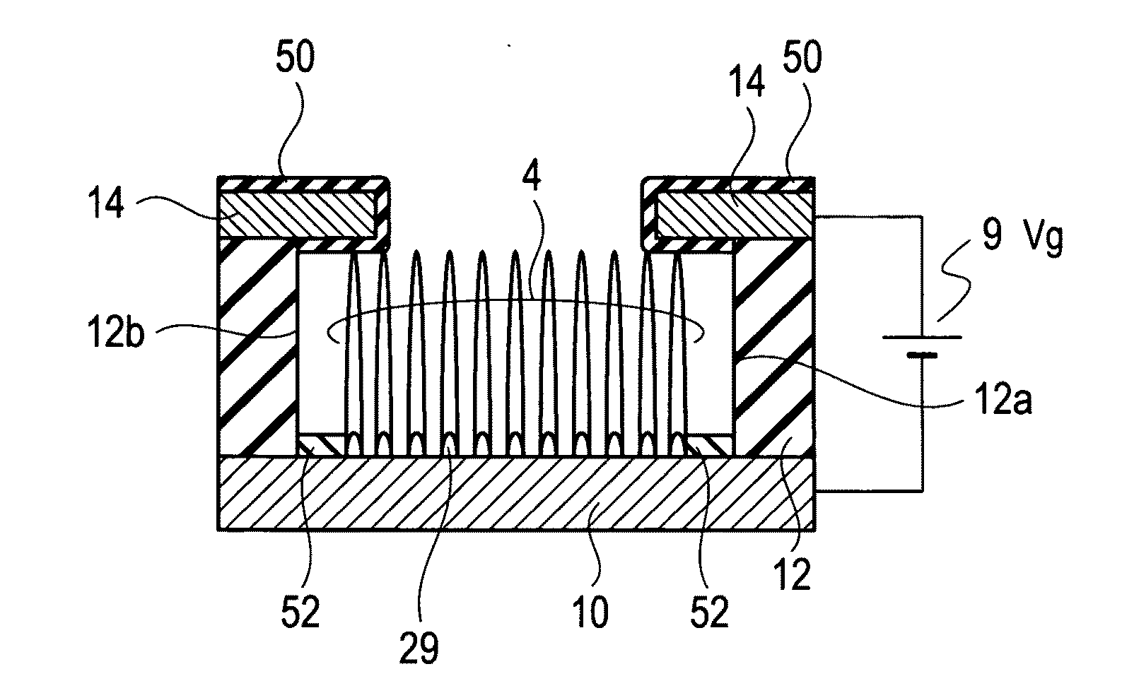
[0074]A fabrication method for carbon fiber according to a first embodiment of the present invention includes a formation process of minute holes by dry etching, an ultrasonic catalyst plating process, a previous oxidation process and a growing process of a carbon nano-tube. The formation process of minute holes by dry etching is shown in FIG. 9 to FIG. 11 and FIG. 13A to FIG. 13B. The ultrasonic catalyst plating process is shown in FIG. 12 and FIG. 13C. The previous oxidation process and the growing process of the carbon nano-tube are shown in FIG. 13D and FIG. 14.

[0075]An experimental result by the fabrication method for carbon fiber according to the first embodiment of the present invention is as being shown in FIG. 15 to FIG. 22.

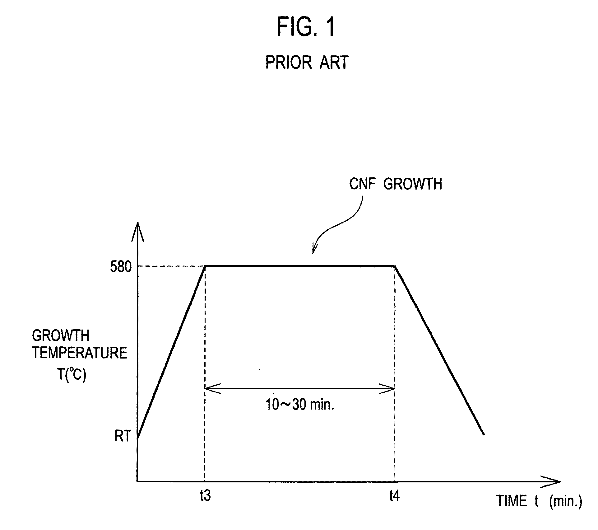
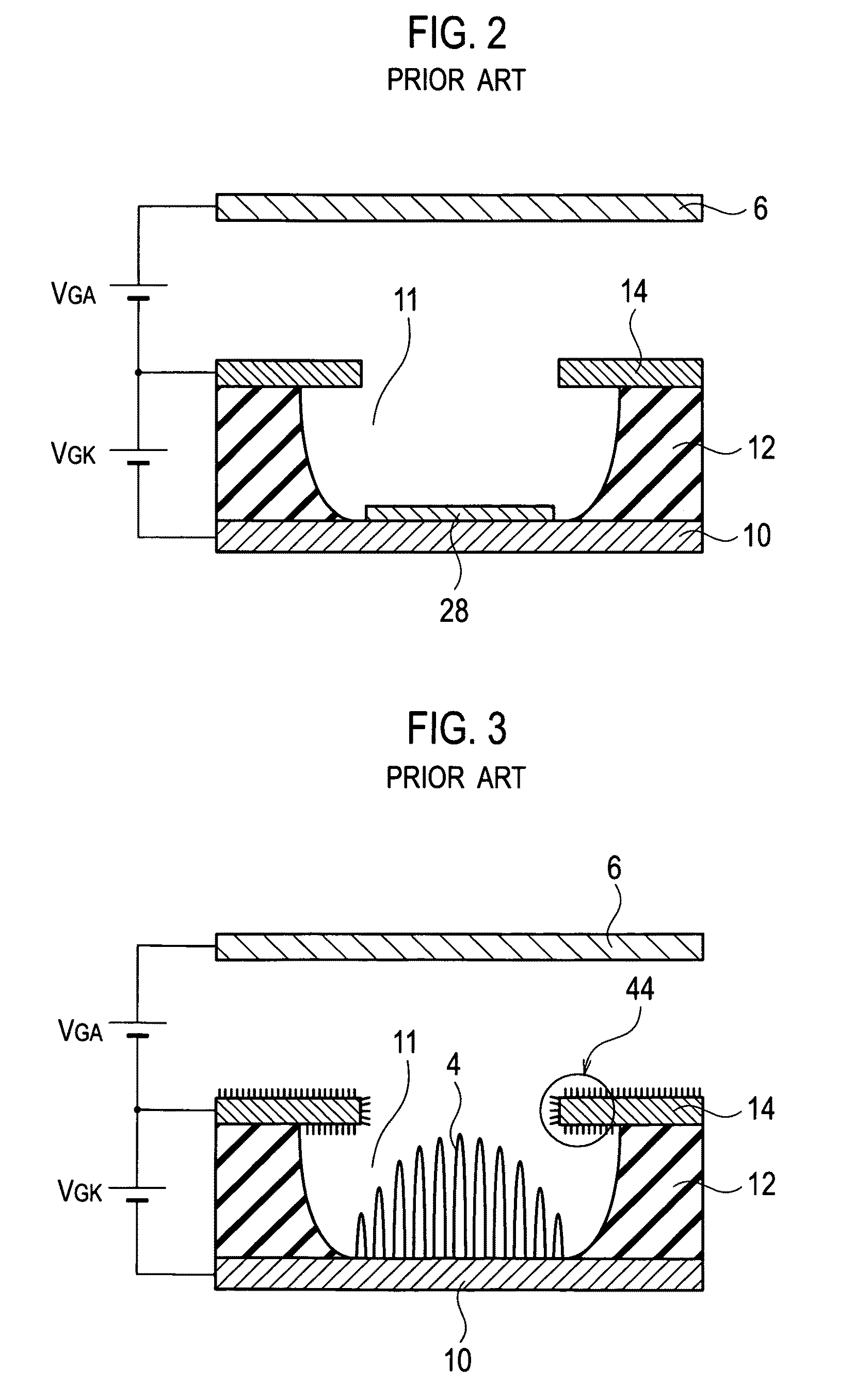
[0076]The fabrication method for carbon fiber according to the first embodiment of the present invention has the characteristic at a point of performing the previous oxidation process, at the time of growth of carbon...


PUM

PropertyMeasurementUnit
depthaaaaaaaaaa
depthaaaaaaaaaa
aspect ratioaaaaaaaaaa

Abstract

A fabrication method for carbon fiber which can prevent abnormal growth from electrode wiring metal, and can be formed a carbon nano-tube with high-density and uniform, by a simple and cheap method and the fabrication method includes process steps: forming a cathode electrode on a substrate; forming a first insulating film on the cathode electrode; forming a gate electrode on the first insulating film; forming a hole which reaches to the cathode electrode surface into the first insulating film; forming a catalyst crystallite nucleus on a bottom of the hole; oxidized forming a second insulating film on the gate electrode surface; and forming a carbon nano-tube on the catalyst crystallite nucleus; a carbon fiber electron source of high-output current density; and FED device which has high-intensity and large capacity with high current density, are provided.

Description

CROSS REFERENCE TO RELATED APPLICATION AND INCORPORATION BY REFERENCE[0001]This application is based upon and claims the benefit of priority from prior Japanese Patent Application No. P2007-216140 filed on Aug. 22, 2007, the entire contents of which are incorporated herein by reference.BACKGROUND OF THE INVENTION[0002]1. Field of the Invention[0003]The present invention relates to a fabrication method for a carbon fiber, and in particular, relates to a fabrication method for a carbon fiber for preventing abnormal growth by electrode oxidation, and a carbon fiber electron source and an FED (Field Emission Display) devices which apply the fabricated carbon fiber.[0004]2. Description of the Related Art[0005]In a fabrication method of the conventional carbon nano-tube, a catalyst is formed by sputtering in a hole by using a resist as a mask (for example, refer to Patent Document 1.). Furthermore, it is necessary to perform lift off of the resist after catalyst sputtering (for example, r...

Claims


Application Information

Patent Timeline
Patent Type & Authority Applications(United States)
IPC IPC(8): H01J1/62H01J19/06H01J9/04
CPCH01J9/025H01J2329/0455H01J2329/0431H01J2329/0428
Inventor KATO, TOMOHIRO
Owner ROHM CO LTD
Why Eureka
Try Eureka