Nanoscale Wire-Based Data Storage

Inactive Publication Date: 2009-04-16
PRESIDENT & FELLOWS OF HARVARD COLLEGE
View PDF99 Cites 35 Cited by
  • Summary
  • Abstract
  • Description
  • Claims
  • Application Information

AI Technical Summary

Benefits of technology

[0018]In another aspect, the present invention is directed to a method of making one or more of the embodiments described herein. In yet another aspect, the present invention is directed to a method of using one or more of the embodiments described herein.
[0019]Other advantages and novel features of the present invention will become apparent from the following detailed description of various non-limiting embodiments of the inventi

Problems solved by technology

While nanoscopic articles might be well-suited for transport of charge carriers and excitons (e.g. electrons, electron-hole pairs, electron pairs, etc.) and th

Method used


Image

  • Nanoscale Wire-Based Data Storage
  • Nanoscale Wire-Based Data Storage
  • Nanoscale Wire-Based Data Storage

Examples


example 1

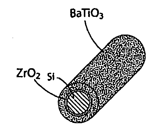
[0110]This example demonstrates the synthesis of semiconductor / dielectric oxide / ferroelectric oxide core / shell / shell nanoscale wire structure, specifically p-Si / ZrO2 / BaTiO3 core / shell / shell nanoscale wires (FIG. 1A), according to one embodiment of the invention. In this example, the shells were fabricated using ALD techniques (atomic layer deposition), but other techniques, for example, solution-based approaches, can be used as well.

[0111]The synthesis starts from chemical vapor deposition growth of p-type silicon nanoscale wires using gold colloids as a catalyst, silane as a reactant, and diborane as a dopant in the well-known VLS growth process. After growth, the growth wafer was transferred directly into an atomic layer deposition reactor. ZrO2 high-K dielectric oxide was deposited onto the Si nanoscale wires to make p-Si / ZrO2 core / shell nanoscale wires by using ZrCl4 as a Zr source and water vapor as an oxygen source. ZrO2 can function as a high-K dielectric, which can enhance p...

example 2

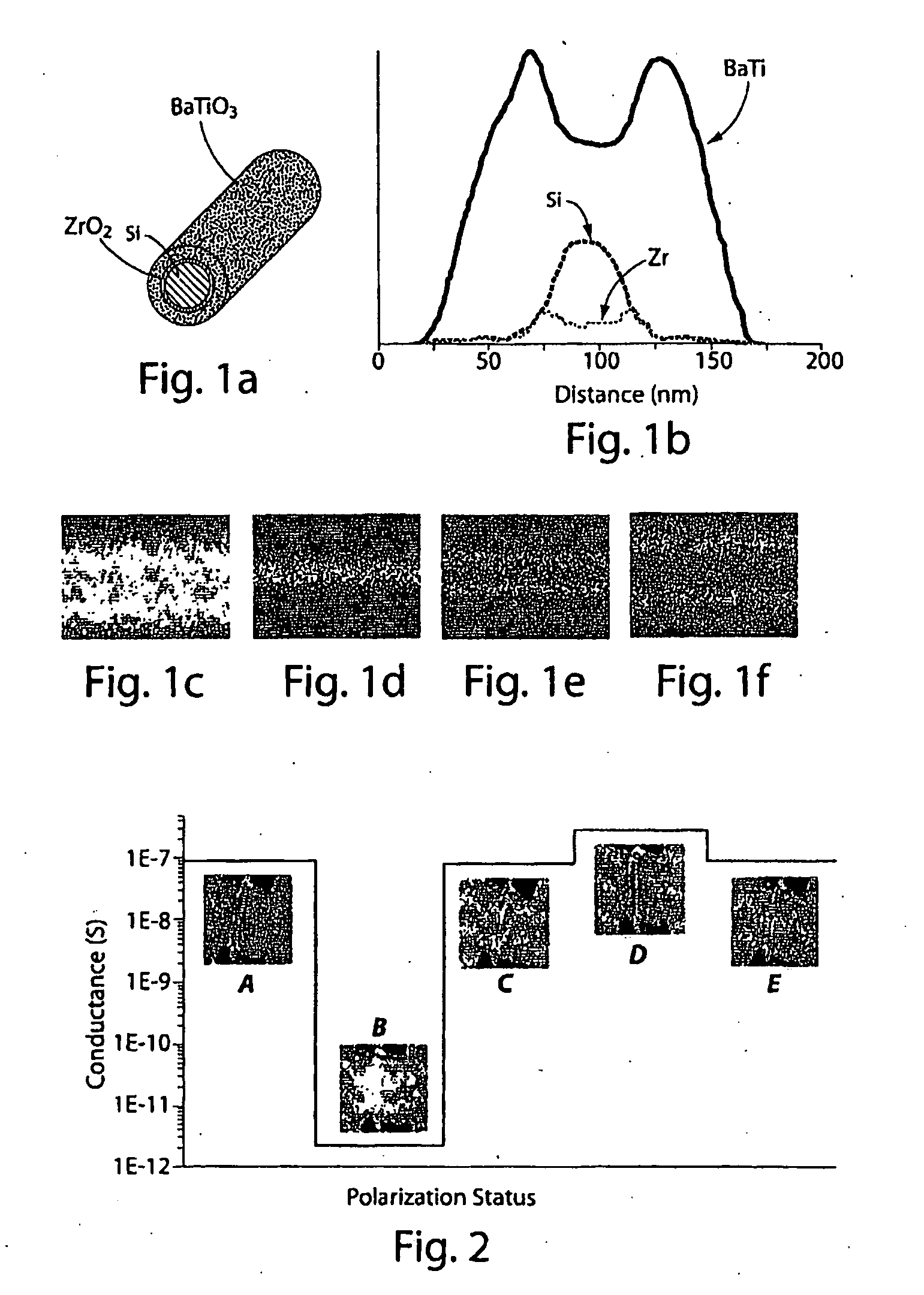
[0120]This example illustrates the fabrication of silicon-functional oxide core-shell nanowire heterostructures by atomic layer deposition (ALD), in which the conformal coating of various materials, including oxides, on silicon nanowires was achieved through cycled self-limiting surface reactions by alternating pulse and purge cycles for different reactants. The thickness of the coating was controlled by the number of deposition cycles down to the atomic scale, and thus, the technique may be suitable for fabricating multi-compositional heterostructures with clean interfaces.

[0121]One of the example structures synthesized was a silicon (Si)-zirconium oxide (ZrO2)-barium titanate (BaTiO3) semiconductor-dielectric oxide-ferroelectric oxide core-shell-shell nanowire heterostructure (FIG. 12). FIG. 12A shows the deposition of functional oxide shells over p-type silicon nanowires. The synthesis started from the growth of p-type Si nanowires by chemical vapor deposition, followed by vapor ...

example 3

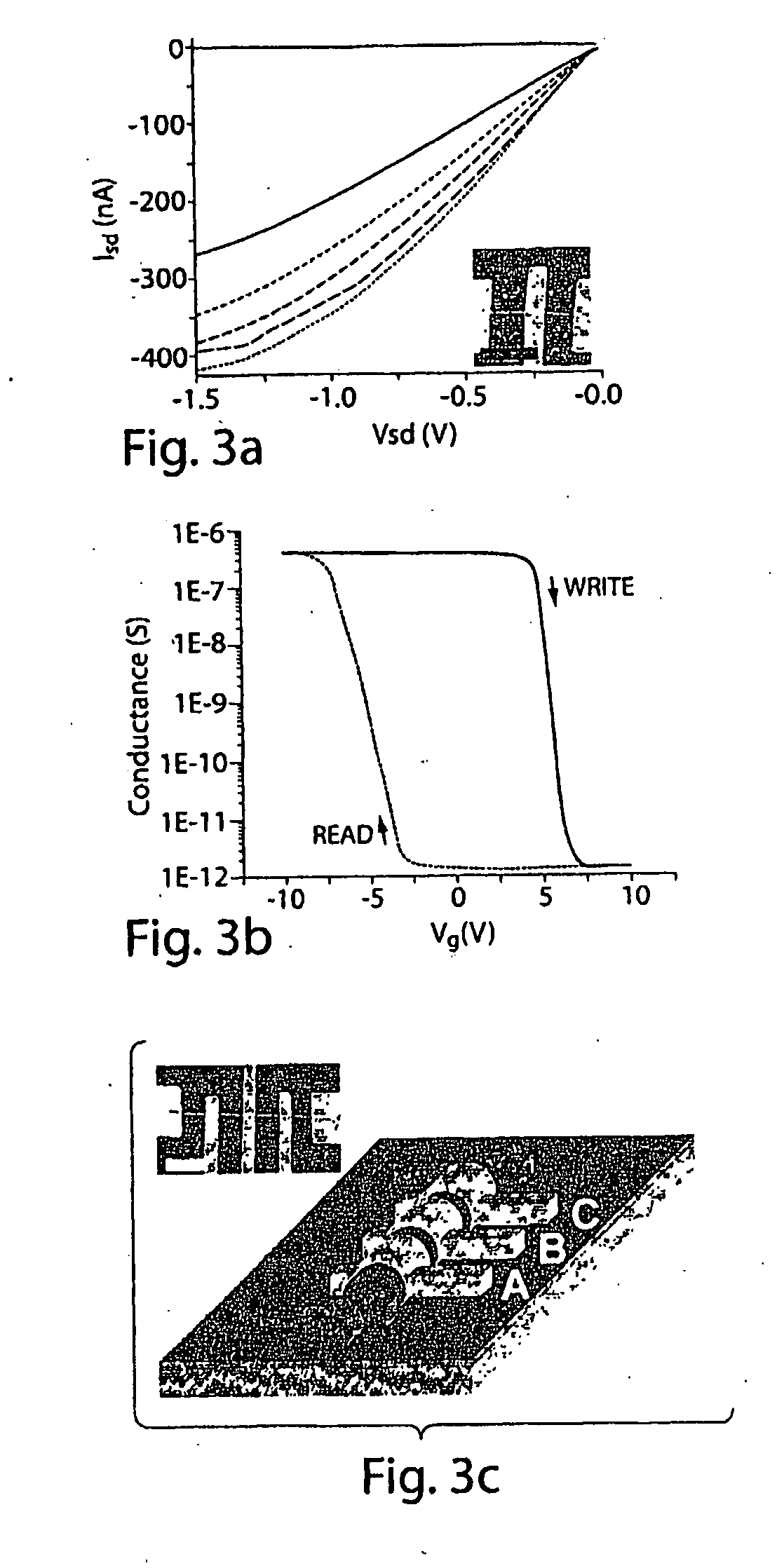
[0127]This example illustrates the synthesis of a well-defined semiconductor-functional oxide core-shell nanowire heterostructure with a clean interface. In this example, a field-effect transistor (FET) device was prepared based on a Si / ZrO2 / BaTiO3 core-shell nanowire heterostructure (FIG. 14). To form the device, the oxides at the source-drain regions were etched away by hydrogen fluoride (HF) acid, followed by deposition of metal contacts on the p-type Si core. A nickel top gate was fabricated between the source-drain contacts on top of the BaTiO3 shell (inset, FIG. 14A, which is a SEM image showing the device geometry, and source-drain contacts having 3 micrometer separation on the p-type Si nanowire core and an 800 nm wide top gate on the top of the BaTiO3 shell in the middle of the channel). The scale bar in the inset is 2 micrometers. Transport results of current (Isd) versus source-drain voltage (Vsd) data (FIG. 14A) at different gate voltages (Vgs) obtained from a core-shell...


PUM


Abstract

The present invention generally relates to nanotechnology and submicroelectronic devices that can be used in circuitry and, in some cases, to nanoscale wires and other nanostructures able to encode data. One aspect of the invention provides a nanoscale wire or other nanostructure having a region that is electrically-polarizable, for example, a nanoscale wire may comprise a core and an electrically-polarizable shell. In some cases, the electrically-polarizable region is able to retain its polarization state in the absence of an external electric field. All, or only a portion, of the electricallypolarizable region may be polarized, for example, to encode one or more bits of data. In one set of embodiments, the electrically-polarizable region comprises a functional oxide or a ferroelectric oxide material, for example, BaTiO3, lead zirconium titanate, or the like. In some embodiments, the nanoscale wire (or other nanostructure) may further comprise other materials, for example, a separation region separating the electricallypolarizable region from other regions of the nanoscale wire. For example, in a nanoscale wire, one or more intermediate shells may separate the core from the electricallypolarizable shell.

Description

RELATED APPLICATIONS[0001]This application claims the benefit of U.S. Provisional Patent Application Ser. No. 60 / 633,733, filed Dec. 6, 2004, entitled “Nanoscale Wire Based Data Storage,” by Lieber, et al., which is incorporated herein by reference.FEDERALLY SPONSORED RESEARCH[0002]Various aspects of the present invention were sponsored by DARPA, Grant Nos. N-00014-01-1-0651 and N00014-04-1-0591. The U.S. Government may have certain rights in the invention.FIELD OF INVENTION[0003]The present invention generally relates to nanotechnology and sub-microelectronic devices that can be used in circuitry and, in particular, to nanoscale wires and other nanostructures able to encode data.BACKGROUND[0004]Interest in nanotechnology, in particular sub-microelectronic technologies such as semiconductor quantum dots and nanowires, has been motivated by the challenges of chemistry and physics at the nanoscale, and by the prospect of utilizing these structures in electronic, optical, and related d...

Claims


Application Information

Patent Timeline
IPC IPC(8): H01L45/00
CPCB82Y10/00H01L29/78391G11C11/22G11C11/223G11C11/54G11C11/56G11C11/5657G11C13/003G11C13/025G11C2213/16G11C2213/17G11C2213/18G11C2213/75G11C2213/77H01L29/0665H01L29/0673H01L29/068B82Y30/00G11B9/02
Inventor LIEBER, CHARLES M.WU, YUEYAN, HAO
Owner PRESIDENT & FELLOWS OF HARVARD COLLEGE
Why Eureka
Try Eureka