

Circuit board and semiconductor module using this, production method for circuit board
a production method and circuit board technology, applied in the field of circuit boards, can solve the problems of poor electrical isolation, cracking of insulating-ceramic substrates, high thermal stress in cooling processes, etc., and achieve high fracture toughness values, high endurance, and strong correlation
- Summary
- Abstract
- Description
- Claims
- Application Information
AI Technical Summary
Benefits of technology
Problems solved by technology
Method used
Image

Examples
1st embodiment
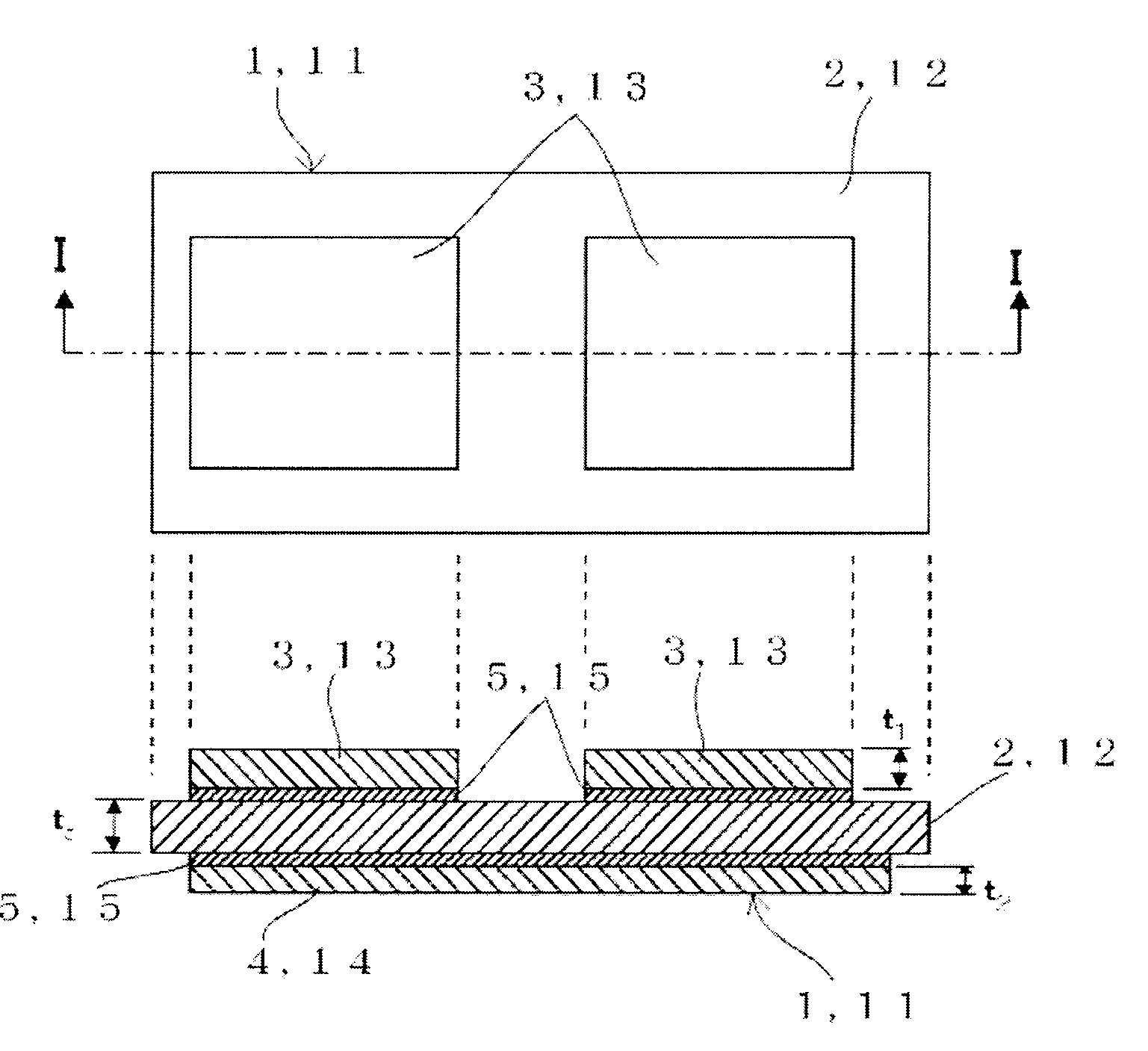
[0047]Especially a circuit board concerning a 1st embodiment of this invention is effective when the strongly anisotropic insulating-ceramic substrate is used. The top view of this circuit board 1 and the cross sectional view in I-I direction are shown in FIG. 1. In this circuit board 1, metal circuit plate 3 and metal heat sink 4 are bonded to one face and to another face respectively, of the insulating-ceramic substrate 2, via brazing material 5. As insulating-ceramic substrate 2, silicon nitride ceramics are used, for example. Copper is used as metal circuit plate 3 and metal heat sink 4, and the brazing material 5 is composed of an active metal, typically Ag—Cu system alloy to which Ti is doped for example, and by using this, the metal circuit plate 3 and the heat sink 4 are bonded to the insulating-ceramic substrate 2 at the temperature of about 750° C. A semiconductor module using this circuit board 1 is formed by bonding and mounting a semiconductor chip (not shown) with sold...
2nd embodiment
[0062]The circuit board 11 concerning a 2nd embodiment of this invention can be applied irrespective of degree of the anisotropy of the insulating-ceramic substrate. The structure of this circuit board 11 is similar to that of the circuit board 1 concerning a 1st aforementioned embodiment, and that top view and the sectional view in I-I direction are shown in FIG. 1. In this circuit board 11, the metal circuit plate 13 and the metal heat sink 14 are bonded to one face and to another face respectively, of the insulating-ceramic substrate 12, via metal brazing material 15. Here, the thickness of the insulating-ceramic substrate 12 is shown as “tc”, the thickness of the metal circuit plate 13 is shown as “t1”, and the thickness of the metal heat sink 14 is shown as “t2”. The thickness of the brazing material 15 is negligibly small to them. As insulating-ceramic substrate 12, silicon nitride ceramics is used, for example. As metal circuit plate 13 and metal heat sink 14, copper is used,...
example
[0079]Hereafter, the example of this invention is described. However, this invention is not limited by these examples.
[0080]Using silicon nitride ceramics substrates as insulating-ceramic substrates, and using copper plates as metal circuit plates and as metal heat sinks, circuit boards and semiconductor modules were produced. In-plane fracture toughness values K, internal fracture toughness values KH, and thickness of the silicon nitride ceramics substrates, and thickness of the metal circuit plates and the metal heat sinks, are shown in Table 1.
[0081]Active metal brazing materials were printed on both faces of the silicon nitride ceramic substrates, and copper plates with almost same rectangular shape as the silicon nitride substrates were heated and bonded to the both faces of silicon nitride ceramic substrates at temperature of 600-900° C. Each temperature (bonding temperature) is shown in Table 1. After cooling, these were etched so that the metal circuit plates and the metal h...
PUM
| Property | Measurement | Unit |
|---|---|---|
| bonding temperature | aaaaa | aaaaa |
| temperature | aaaaa | aaaaa |
| thickness | aaaaa | aaaaa |
Abstract
Description
Claims
Application Information