

Light transmitting conductive film, light transmitting electromagnetic wave shielding film, optical filter and method of producing display filter
- Summary
- Abstract
- Description
- Claims
- Application Information
AI Technical Summary
Benefits of technology
Problems solved by technology
Method used
Image

Examples
example 1-1
Silver Halide Photosensitive Material
[0397]An emulsion containing 10.0 g of gelatin to 60 g of Ag in an aqueous medium and containing silver iodobromide grains (I=0.2% by mol, Br=40% by mol) having a sphere-corresponding average diameter of 0.1 μm was prepared.
[0398]In this emulsion, K3Rh2Br9 and K2IrCl6 were added to give a concentration of 10−7 mol / mol of Ag thereby doping the silver bromide grains with Rh ions and Ir ions. To this emulsion, Na2PdCl4 was added and a gold-sulfur sensitization was conducted with the use of chloroauric acid and sodium thiosulfate. Next, the emulsion was coated together with a gelatin film hardening agent on the polyethylene terephthalate (PET) to give a silver coating amount of 1 g / m2. In this step, the Ag / gelatin volume ratio was adjusted to ½.
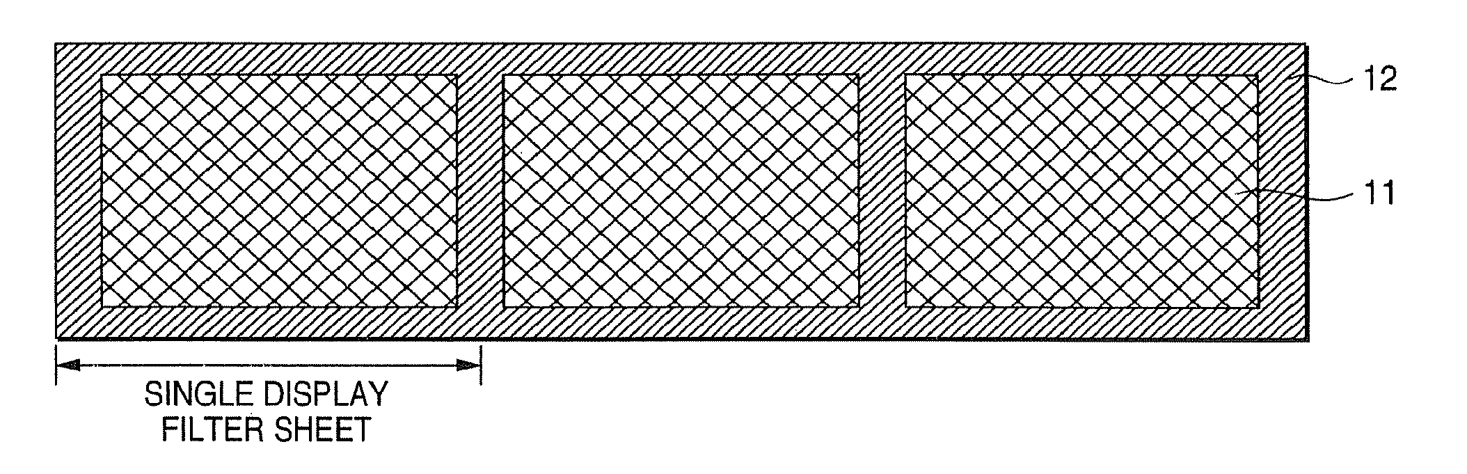
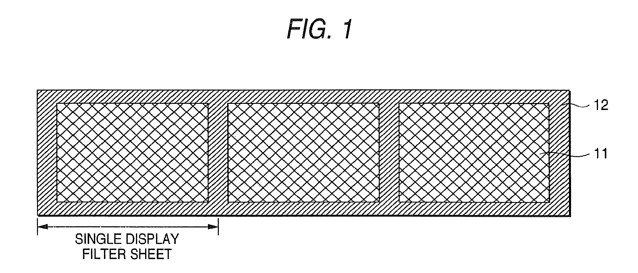
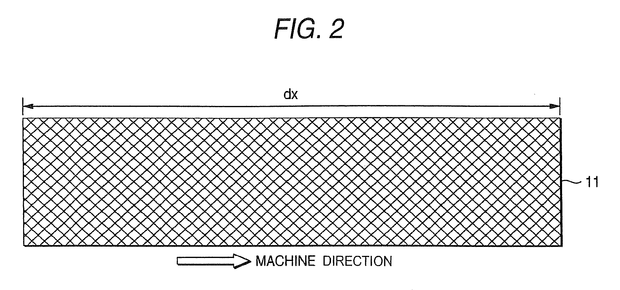
[0399]The emulsion was coated on a part (25 cm in width, 20 m in length) of a PET support having a width of 30 cm. Then the both edges (3 cm) of the support were cut off while remaining the center (24 cm) of t...
example 1-2
[0414]As a typical example of “(3) Mesh obtained by etching process using photolithographic technique” cited in the above Background Art, a metal mesh disclosed in JP-A-2003-46293 was manufactured.
[0415]When compared as in Example 1-1, it was clarified that an even surface resistivity was obtained by forming the continuous pattern according to the present invention, which indicates the effectiveness of the invention.
example 1-3
[0416]Sample C was produced as in Sample A in Example 1-1 but the continuous pattern was formed by conducting the exposure with the use of a rotational polygon mirror scanning laser exposure which was located so as to conduct scanning at angles of 45° and −45° to the transport direction of the silver halide photosensitive material. When Sample C was compared with Sample B, the same results as in Example 1-1 were obtained.
PUM
| Property | Measurement | Unit |
|---|---|---|
| Length | aaaaa | aaaaa |
| Length | aaaaa | aaaaa |
| Length | aaaaa | aaaaa |
Abstract
Description
Claims
Application Information