Conductive Filler and Solder Material

a technology of soldering material and conductive filler, which is applied in the direction of soldering apparatus, manufacturing tools, and capacitors, etc., can solve the problems of limited use of au—sn based metal alloys, lead harm, and high cost of materials, and achieve high temperature resistan

Active Publication Date: 2009-06-04
ASAHI KASEI E-MATERIALS CORPORATION +1
View PDF3 Cites 18 Cited by
  • Summary
  • Abstract
  • Description
  • Claims
  • Application Information

AI Technical Summary

Benefits of technology

[0021]The conductive filler of the present invention can be melt-bonded under reflow heat treatment conditions for a lead-free solder, for example, at a peak temperature of 246° C., and, after the bonding, exhibits high temperature resistance such that it do...

Problems solved by technology

However, in recent years, the harmfulness of lead is becoming a problem as described in the EU's environmental regulations (WEEE and RoHS directives), and the percentage of a lead-free solder in the total solder is rapidly increasing from the viewpoint of preventing environmental pollution.
However, the Au—Sn based metal alloy is limited in use because it is a material which is mechanically hard and brittle and thereby has poor stress relaxation characteristics, and it is also an extremely expensive material.
Further, the Sb—Sn based metal alloy is pointed out that it has a...

Method used


Image

  • Conductive Filler and Solder Material
  • Conductive Filler and Solder Material
  • Conductive Filler and Solder Material

Examples


example 1

[0053](1) Production of First Metal Particles

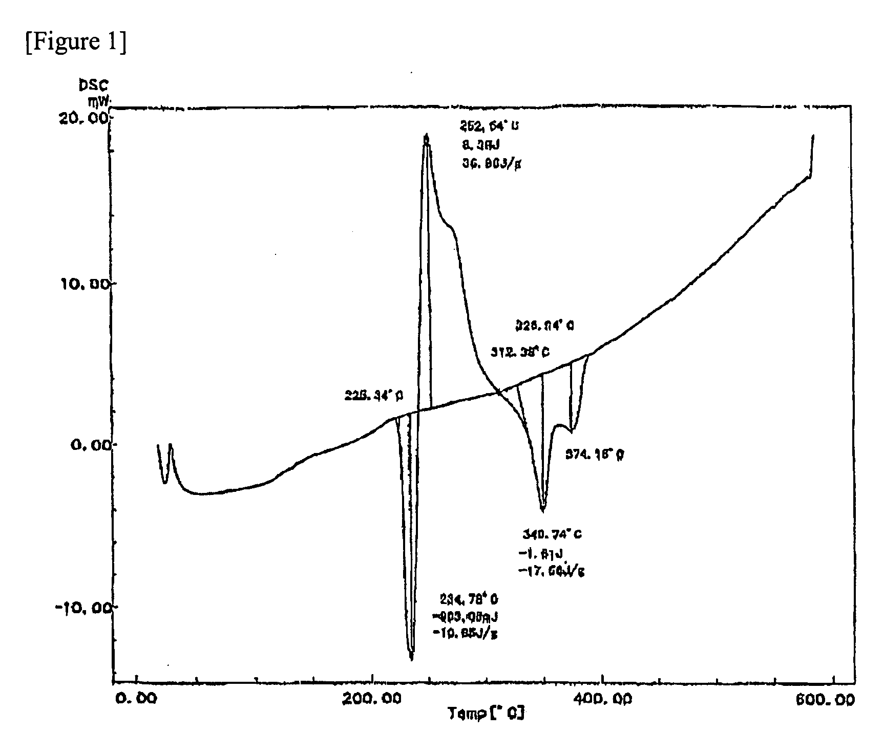
[0054]In a graphite crucible, were placed 6.5 kg of Cu particles (purity: 99% by weight or more), 1.5 kg of Sn particles (purity: 99% by weight or more), 1.0 kg of Ag particles (purity: 99% by weight or more), 0.5 kg of Bi particles (purity: 99% by weight or more), and 0.5 kg of In particles (purity: 99% by weight or more). Using a high frequency induction heater, the mixture in the graphite crucible was heated under an atmosphere of helium gas (purity: 99% by volume or more) so that the temperature of the mixture became 1,400° C., thereby melting the mixture to obtain a molten metal. Next, the molten metal obtained was poured over the brim of the crucible into a spray vessel having an atmosphere of helium gas. From a gas nozzle provided around the brim of the crucible, helium gas (purity: 99% by volume or more; oxygen content: less than 0.1% by volume; pressure: 2.5 MPa) was blown onto the molten metal to gas-atomize the molten metal, th...

example 2

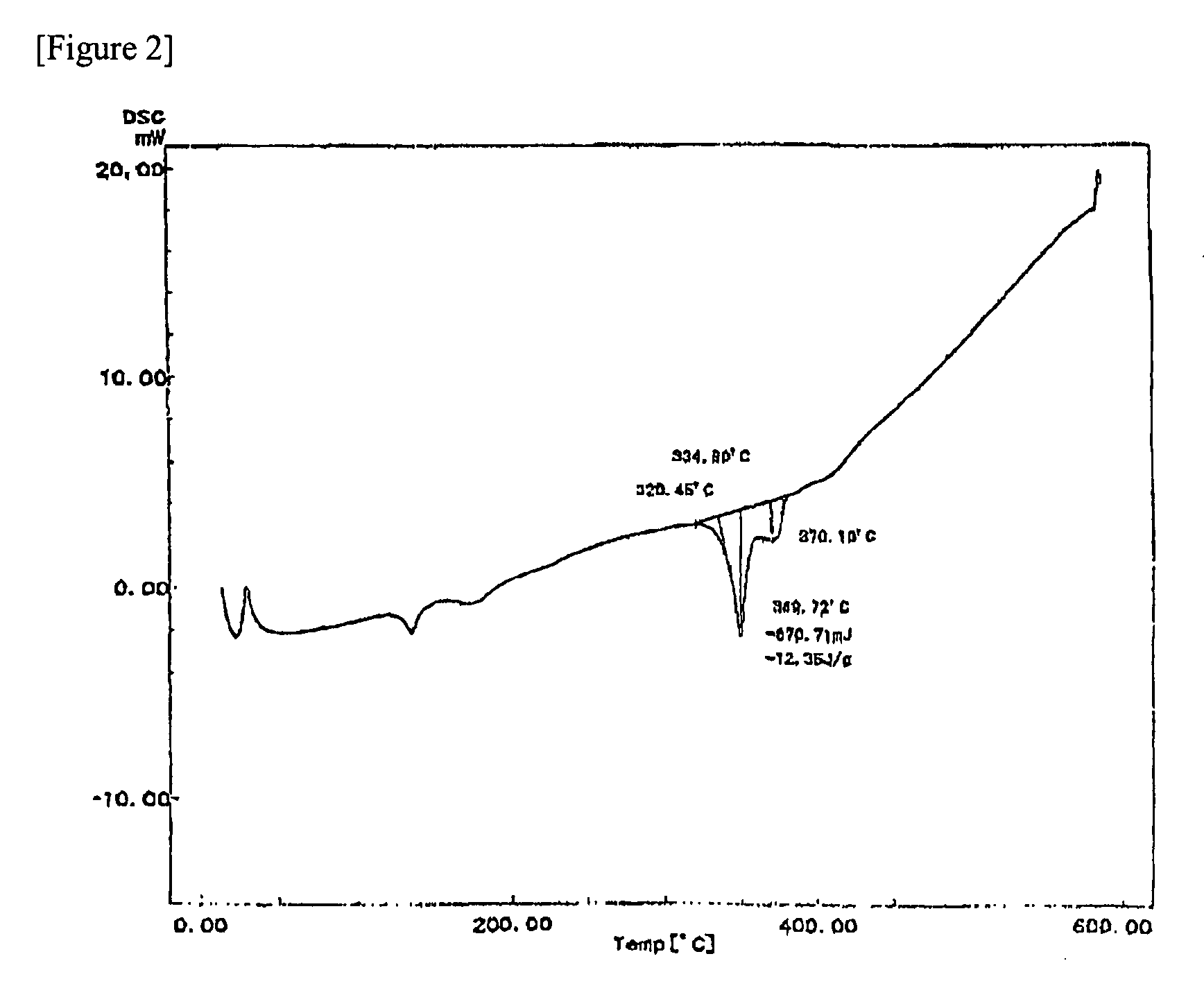
[0068]The first metal particles and the second metal particles before classification prepared by gas atomization in Example 1 were classified by using a current classifier (TC-15N: manufactured by Nisshin Engineering Co., Ltd.) at a setting of 40 μm, followed by collecting the undersize particles. A conductive filler (average particle diameter: 4.7 μm) obtained by mixing the first metal particles and the second metal particles thus obtained at a weight ratio of 100:83 was used as a sample.

[0069]Next, a soldering paste was prepared by mixing 91.5% by mass of the above-mentioned conductive filler, 5.95% by mass of a rosin type flux, 1.7% by mass of triethanolamine (oxide film remover), and 0.85% by mass of hexylene glycol (solvent), and treating the mixture with a kneader equipped with a vacuum deaerator, a three roll mill, and a kneader equipped with a vacuum deaerator in succession.

[0070]The above-mentioned soldering paste was printed on a Cu substrate to thereby form a soldering pa...
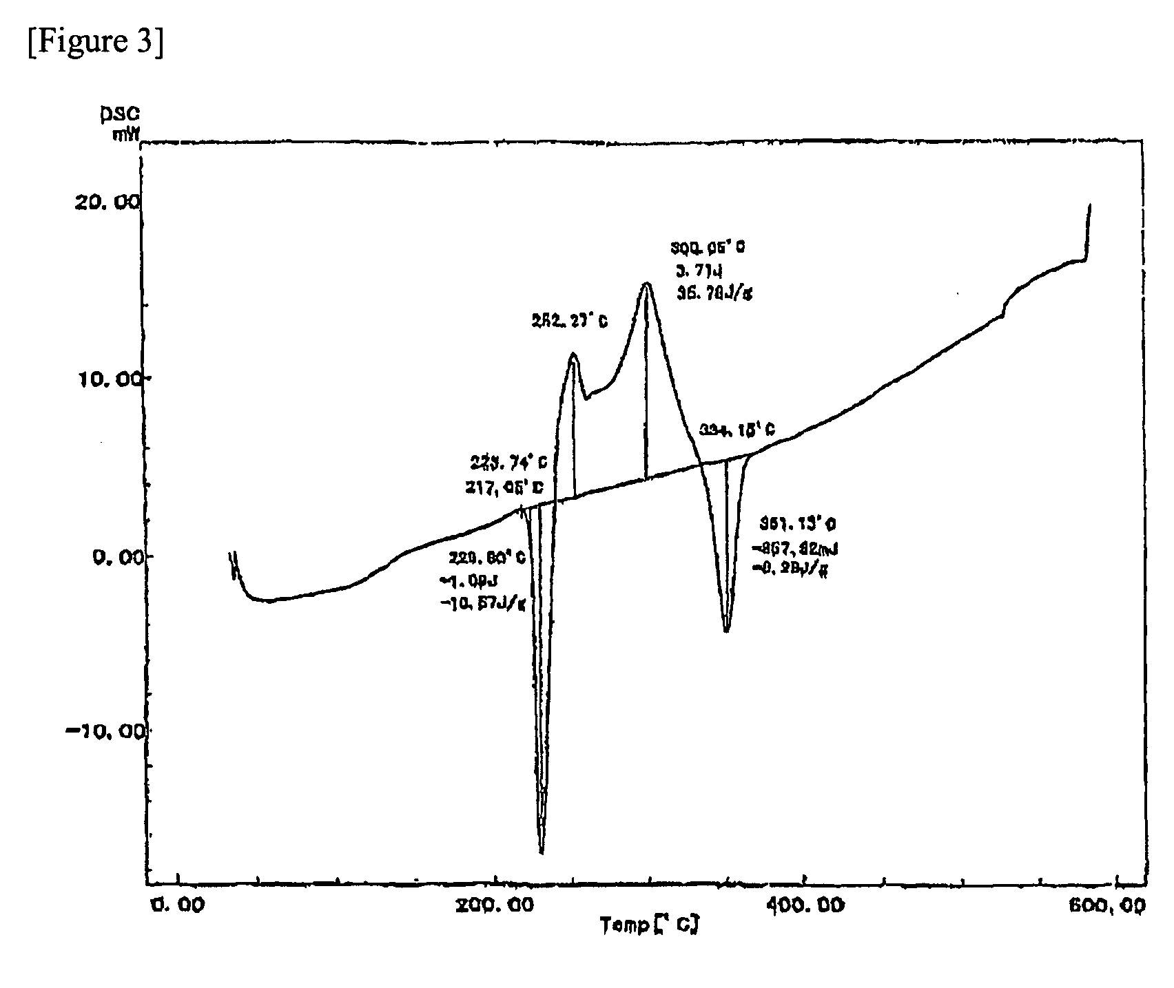
example 3

[0078]A conductive filler (average particle diameter: 4.7 μm) obtained by mixing the first metal particles and the second metal particles classified in Example 2 at a weight ratio of 100:55 was used as a sample for differential scanning calorimetry. The DSC chart obtained by the calorimetry is shown in FIG. 3. As shown in FIG. 3, it was confirmed that the sample exhibited endothermic peaks at 230° C. and 351° C. The endothermic peak at 230° C. corresponds to the melting point of 224° C., and the endotherm is 10.6 J / g. In addition, the sample characteristically exhibited exothermic peaks at 253° C. and 300° C.

[0079]Next, a soldering paste was prepared by mixing 91.5% by mass of the above-mentioned conductive filler, 4.25% by mass of a rosin type flux, 1.7% by mass of triethanolamine (oxide film remover), and 2.55% by mass of hexylene glycol (solvent), and treating the mixture with a kneader equipped with a vacuum deaerator, a three roll mill, and a kneader equipped with a vacuum deae...


PUM

PropertyMeasurementUnit
Temperatureaaaaaaaaaa

Abstract

There is provided a conductive filler with high heat resistance which can be melt-bonded under reflow heat treatment conditions for a lead-free solder and, after the bonding, does not melt under the same heat treatment conditions. The conductive filler is characterized in that, as measured by differential scanning calorimetry, it has at least one metastable metal alloy phase observed as an exothermic peak and has at least one melting point observed as an endothermic peak in each of the 210 to 240° C. range and the 300 to 450° C. range, and that the filler, upon heat treatment at 246° C., gives a bonded object which has, as measured by differential scanning calorimetry, no melting point observed as an endothermic peak in the 210 to 240° C. range or has a melting endotherm calculated from an endothermic peak area in the 210 to 240° C. range, the melting endotherm being 90% or less of the melting endotherm of the filler before bonding calculated from an endothermic peak area in the 210 to 240° C. range.

Description

TECHNICAL FIELD[0001]The present invention relates to a conductive filler used as a bonding material for electric and electronic equipment, particularly to a lead-free solder material and a conductive adhesive.BACKGROUND ART[0002]Solder is generally used for bonding metal materials and is composed of a metal alloy material having a melting temperature range (a range from the solidus temperature to the liquidus temperature) of 450° C. or less. A Sn-37Pb eutectic solder having a melting point of 183° C. has heretofore been generally used as a solder material used in reflow heat treatment. Further, a Sn-90Pb high temperature solder having a solidus temperature of 270° C. and a liquidus temperature of 305° C. has been extensively used as a high temperature solder used in the interior of electronic parts and the like where high heat resistance is required.[0003]However, in recent years, the harmfulness of lead is becoming a problem as described in the EU's environmental regulations (WEEE...

Claims


Application Information

Patent Timeline
IPC IPC(8): B23K35/22H01B1/02B22F1/10
CPCB22F1/0059B23K35/025H05K2201/0272B23K35/302H05K3/3484B23K35/262H05K3/3485B22F1/10B23K35/383C22C9/00C22C13/00B23K2101/40
Inventor TANAKA, NORIHITOSHIMAMURA, YASUKI
Owner ASAHI KASEI E-MATERIALS CORPORATION
Why Eureka
Try Eureka