Method for diamond surface treatment and device using diamond thin film

a technology of diamond surface treatment and thin film, which is applied in the direction of basic electric elements, electrical apparatus, and semiconductor devices, can solve the problems of insufficient thermal conductivity, difficult to control the height of schottky barrier, and dielectric breakdown voltage, etc., to achieve high reverse voltage, stabilize diode characteristics, and suppress reverse leakage current

Inactive Publication Date: 2009-06-04
NAT INST OF ADVANCED IND SCI & TECH
View PDF2 Cites 4 Cited by
  • Summary
  • Abstract
  • Description
  • Claims
  • Application Information

AI Technical Summary

Benefits of technology

[0029]The diamond power semiconductor element of the present invention is able to suppress the reverse leakage current of devices such as various types of diodes, transistors and thyristors to a lower level, able to stabilize diode characteristics (on-voltage, in particular) which would be otherwise not uniform, and also able to withstand a high reverse voltage when used in various types of power semiconductor circuits. More specific applications of the present invention include diamond power semiconductor elements used in the fields of various types of industrial equipment including high-voltage pulse generators including, for example, electron beam irradiation apparatuses, ion implanters, laser generators, X-ray generators, other particle beams generators, plasma generators;, high-voltage supply equipment for electric trains and automobiles; electricity generating / receiving / transmitting equipment; and household electrical appliances.

Problems solved by technology

Although vertical devices using diamond have been developed, sufficient thermal conductivity, dielectric breakdown voltage, and thermal resistance have not yet been obtained.
Further, the cause of the significant reverse leakage current and countermeasures to reduce the reverse leakage current had not yet been found (Non-patent Document 2).
It is, however, difficult to control the Schottky barrier height and to obtain a barrier with a height of more than 2eV and with excellent reproducibility (Non-patent Documents 4-28).

Method used


Image

  • Method for diamond surface treatment and device using diamond thin film
  • Method for diamond surface treatment and device using diamond thin film
  • Method for diamond surface treatment and device using diamond thin film

Examples


embodiment 1

Fabrication of Schottky Barrier Diode

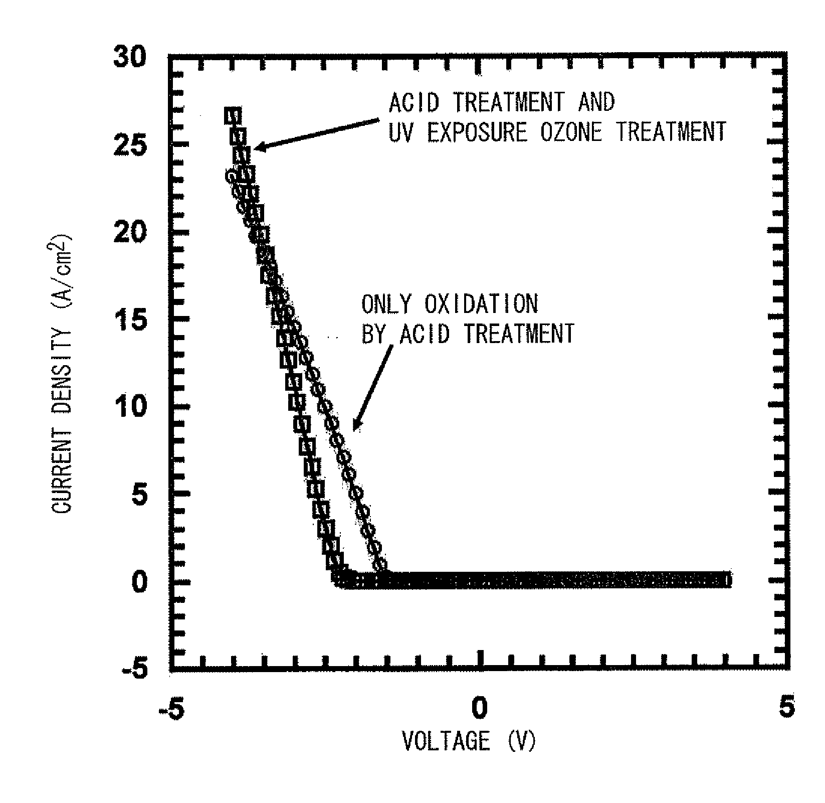
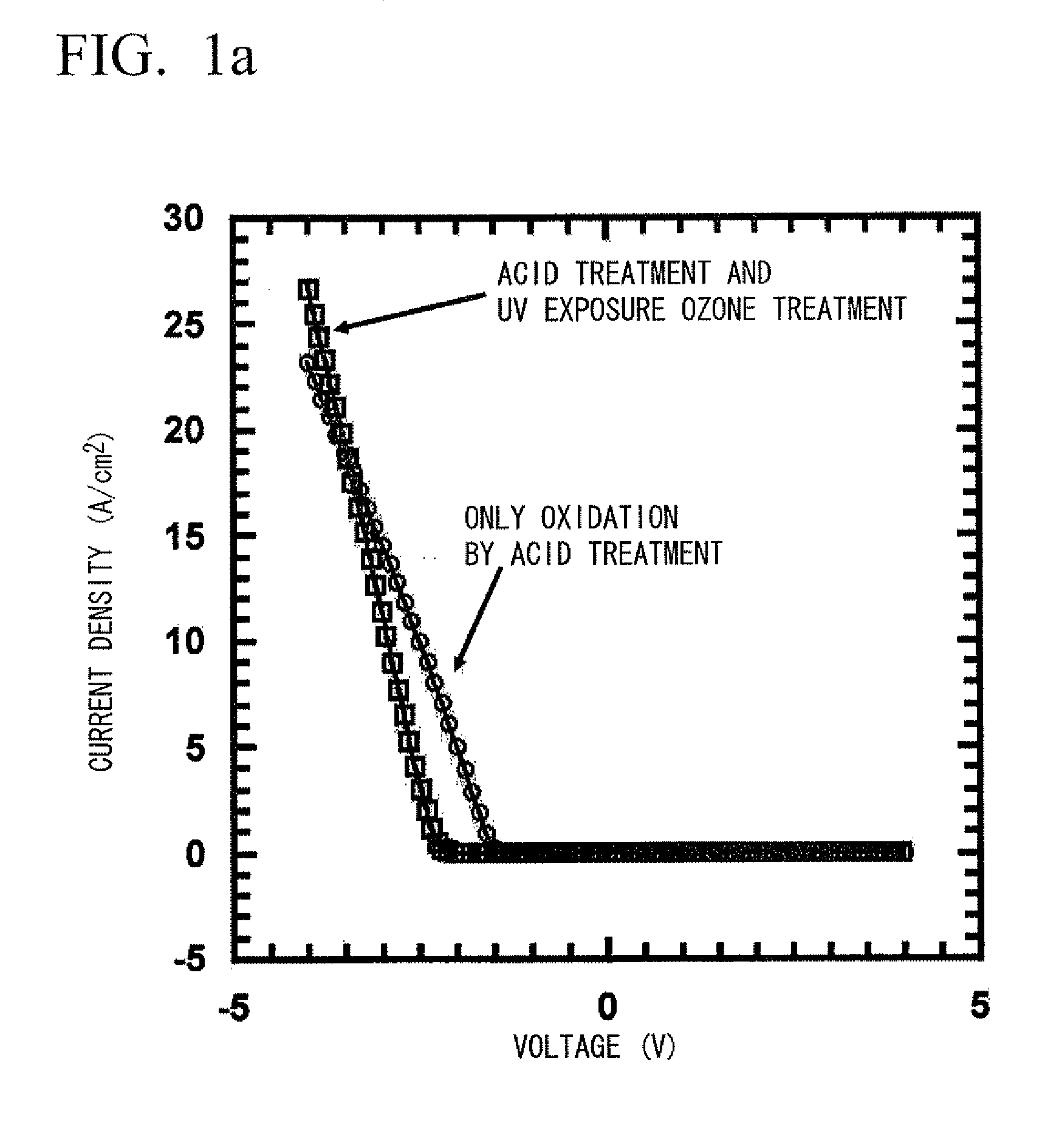
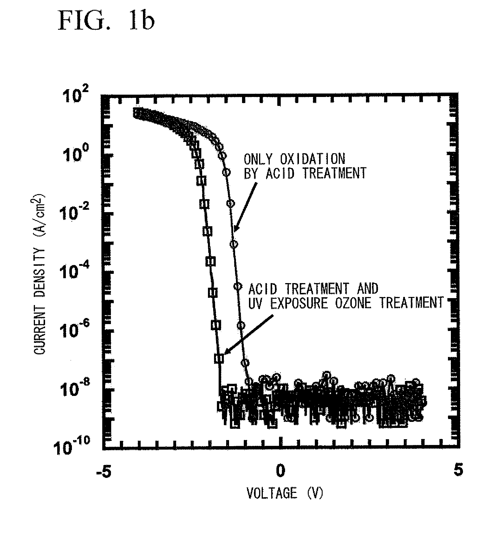
[0051]A low-concentration boron-added homoepitaxial diamond thin film which was formed in a thickness of 1 μm on a high-concentration boron-added diamond single crystal at boron concentrations of 100 ppm to 10 ppm and 1 ppm or lower with respect to carbon inside a reaction tank for microwave CVD method was used as a specimen. The acceptor concentration was 1.5×10¹⁵ to 9×10¹⁶ / cm3. After cleaning of a substrate with hot mixed-acid of nitric acid and hydrochloric acid, a Ti / Pt / Au ohmic electrode was formed on the high-concentration boron-added diamond on the back of the substrate to conduct alloying annealing. Then, in an environment of an oxygen atmosphere of 50% oxygen and 50% nitrogen, the substrate was exposed to UV rays containing wavelengths of 172 nm or 184.9 nm, and 253.7 nm, and UV ray ozone concurrent treatment was conducted on the substrate at 500 ppm to 1000 ppm of ozone formed by UV rays in a ultraviolet ray intensity of 3.7 mW / cm2 for ...

embodiment 2

[0053](1) Quantification of Surface Oxygen Amount

[0054]A substrate subjected to UV ozone treatment was subjected to XPS (X-ray photoelectron spectroscopy) and the amount of oxygen atoms adsorbed on the surface was measured. The measurement found peaks of carbon, oxygen, and silicon. Evaluation was made for coverage by referring to the respective peak area ratios, measurement sensitivity coefficients and mean free path of C1s photoelectrons. FIG. 4 shows a ratio of O1s peak area to C1s peak area by various treatments.

[0055]It is noted that in this measuring apparatus, the ratio of O1s / C1s, or approximately 0.2 was equivalent to approximately 50% of an amount of oxygen adsorbed by the surface of the substrate. The measurement result revealed that in the oxidation treatment by the hot mixed-acid treatment, the ratio of O1s / C1s was from approximately 0.1 to 0.2, but the concentration of oxygen adsorbed on the surface was increased in accordance with an increase in UV ozone treatment tim...

embodiment 3

Example of Mo

[0057]FIG. 6a is a graph showing electric characteristics of devices which have Schottky electrodes including Mo and were subjected to a UV ozone treatment or an ozone treatment according to the present invention. The Schottky barrier height (SBH) was increased in accordance with an increase in the ozone treatment time. The SBH of the elements that had been subjected to ozone free treatment with the use of Mo was 1 to 1.2eV. Where the elements were subjected to the ozone treatment for 3 and 6 hours, the respective SBHs were 1.2eV and 1.4eV. However, when the elements were subjected to the UV ozone treatment, a higher SBH of 2.5eV was observed.

[0058]FIG. 6b shows the reverse characteristics of the elements which were subjected to the ozone treatment for 3 and 6 hours and to the UV ozone treatment. Elements higher in SBH were effectively decreased in leakage current even at a high voltage. Therefore, the elements that were subjected to the UV ozone treatment had a lower l...


PUM

PropertyMeasurementUnit
reverse leakage currentaaaaaaaaaa
wavelengthsaaaaaaaaaa

Abstract

A method for surface treatment of diamond comprising exposing the surface of diamond to UV light containing wavelengths of 172 nm to 184.9 nm and 253.7 nm at an integrated exposure of 10 to 5,000 J/cm2 in an environment of an atmosphere having an oxygen concentration of 20 to 100% and an ozone concentration of 10 to 500,000 ppm to adsorb oxygen on the surface of diamond.

Description

TECHNICAL FIELD[0001]A diamond semiconductor device manufactured by using a diamond surface treatment method and a diamond thin film of the present invention can be used as a power semiconductor device in the fields of various types of industrial equipment such as high-voltage pulse generators including, for example, electron beam irradiation apparatuses, ion implanters, laser generators, X-ray generators, other particle beams generators, plasma generators; high-voltage supply equipment for electric trains and automobiles; and electricity generating / receiving / transmitting equipment, as well as household electrical appliances.[0002]The diamond power semiconductor device of the present invention enables miniaturization of equipment that handles high voltage, and a reduction in consumption of electricity. Not only will this device replace existing power devices including power devices manufactured from silicon, SiC and GaN but it is also expected to be used in the development of new ap...

Claims


Application Information

Patent Timeline
Patent Type & Authority Applications(United States)
IPC IPC(8): H01L29/16H01L21/22
CPCH01L29/66143H01L29/868H01L29/47H01L21/268H01L29/1602H01L29/872
Inventor UMEZAWA, HITOSHISHIKATA, SHINICHIIKEDA, KAZUHIRO
Owner NAT INST OF ADVANCED IND SCI & TECH
Why Eureka
Try Eureka