Integrated Electronic Sensor

a technology of electronic sensors and integrated sensors, applied in the field of electronic sensors, can solve the problems of reducing delay, low power, and dominated by interconnect delay, and achieve the effects of good response characteristic, fast egress, and sufficient free space volum

Active Publication Date: 2009-06-04
SILICON LAB INC
View PDF29 Cites 70 Cited by
  • Summary
  • Abstract
  • Description
  • Claims
  • Application Information

AI Technical Summary

Benefits of technology

[0011]There are enormous advantages to integrating manufacture of the sensor electrodes and dielectric into the MOS interconnect level manufacture, and to using a Low-K dielectric with an organic polymer instead of being only an oxide. It has been found that such a dielectric allows sufficient ingress of gas or moisture and a good response characteristic.
[0012]In one embodiment, the sensor dielectric material is of a type which thermosets with sufficient free space volume for gas or humidity sensing when cured. Such materials are particularly effective for not only low-temperature deposition in a MOS process, but are excellent as sensor dielectrics.
[0013]In one embodiment, the sensor dielectric material is hydrophobic. This allows fast egress of the small quantity of gas or humidity which ingresses

Problems solved by technology

Most importantly, for battery applications, higher integration generally results in lower power, due to reduced parasitic capacitances.
However the continual shrinking of CMOS transistors means that gate delays are reducing, so that overall delays are now becoming dominated by interconnect delay, especially due to the resistivity of Aluminium and capacitance of silicon dioxide (SiO2, dielectric constant K=4 approx).
In the field of sensors, and in particular wireless sensors, greater integration has been slow because of the difficulties encountered in integration of microcontroller, A-to-D converter (ADC), EEPROM memory, RF transceiver, and sensor elements in the one integrated sensor device.
These difficulties have arisen because of incompatibilities of materials processing for the various elements.
For example, sensor elements have conventionally been manufactured on ceramic or glass substrates and cannot be easily integrated on silicon.
It has also been difficult to integrate RF transceivers, EEPROM / Flash EEPROM memories, and mixed-signal converter circuits on a single CMOS chip, due to the different processes required—bipolar transistors, floating-gates, and poly-poly capacitors, which suffer from substrate parasitics, strain, and mis-match effects.
Also, the aluminium metallisation used in IC processing is prone to corrosion, thus limiting usefulness for some types of sensor applications.
This processing is not amenable to high-volume semiconductor processing, since these are non-standard materials (or even regarded as contaminants) in a modem CMOS fabrication plant.
Therefore they are typically applied in a specialist fabrication plant, or a post-processing operation in a specialist facility, leading to extra cost and production bottlenecks.

Method used


Image

  • Integrated Electronic Sensor
  • Integrated Electronic Sensor
  • Integrated Electronic Sensor

Examples


Embodiment Construction

Brief Description of the Drawings

[0049]The invention will be more clearly understood from the following description of some embodiments thereof given by way of example only with reference to the accompanying drawings in which:

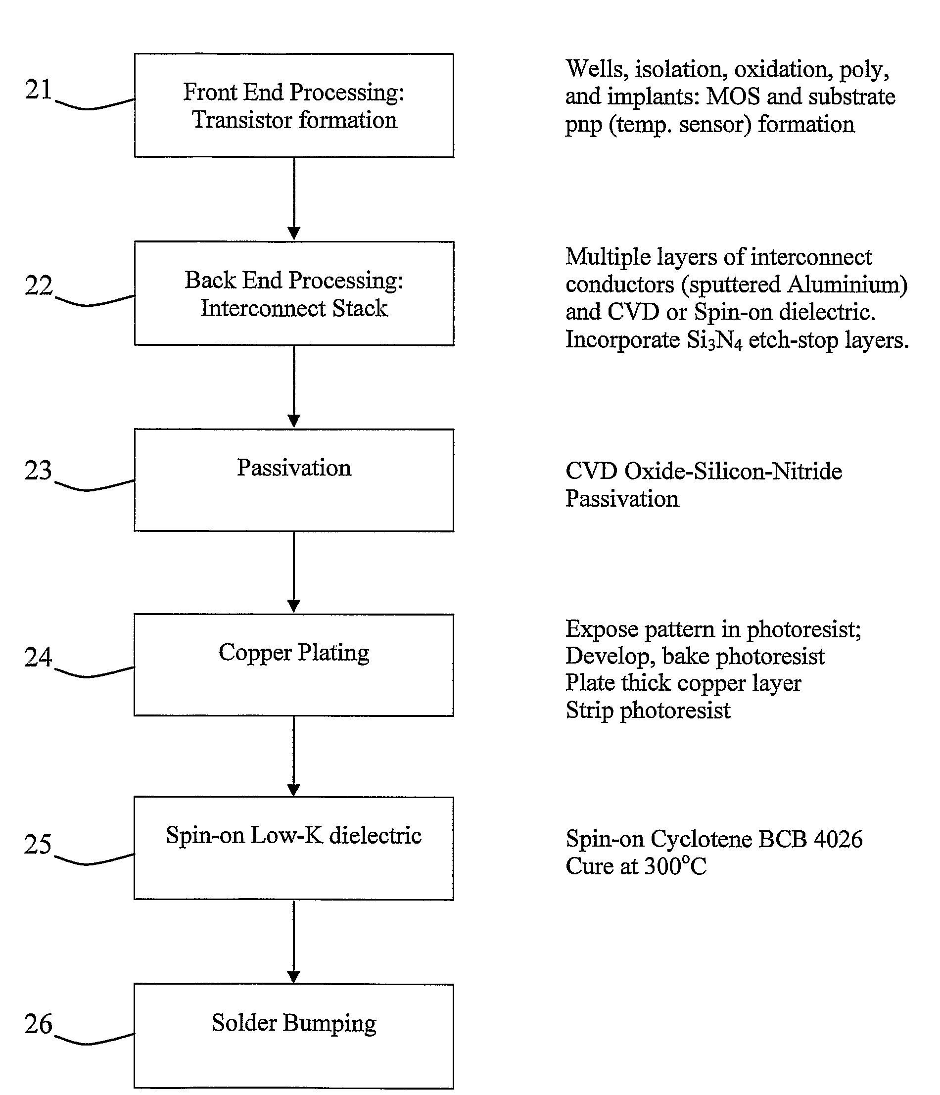
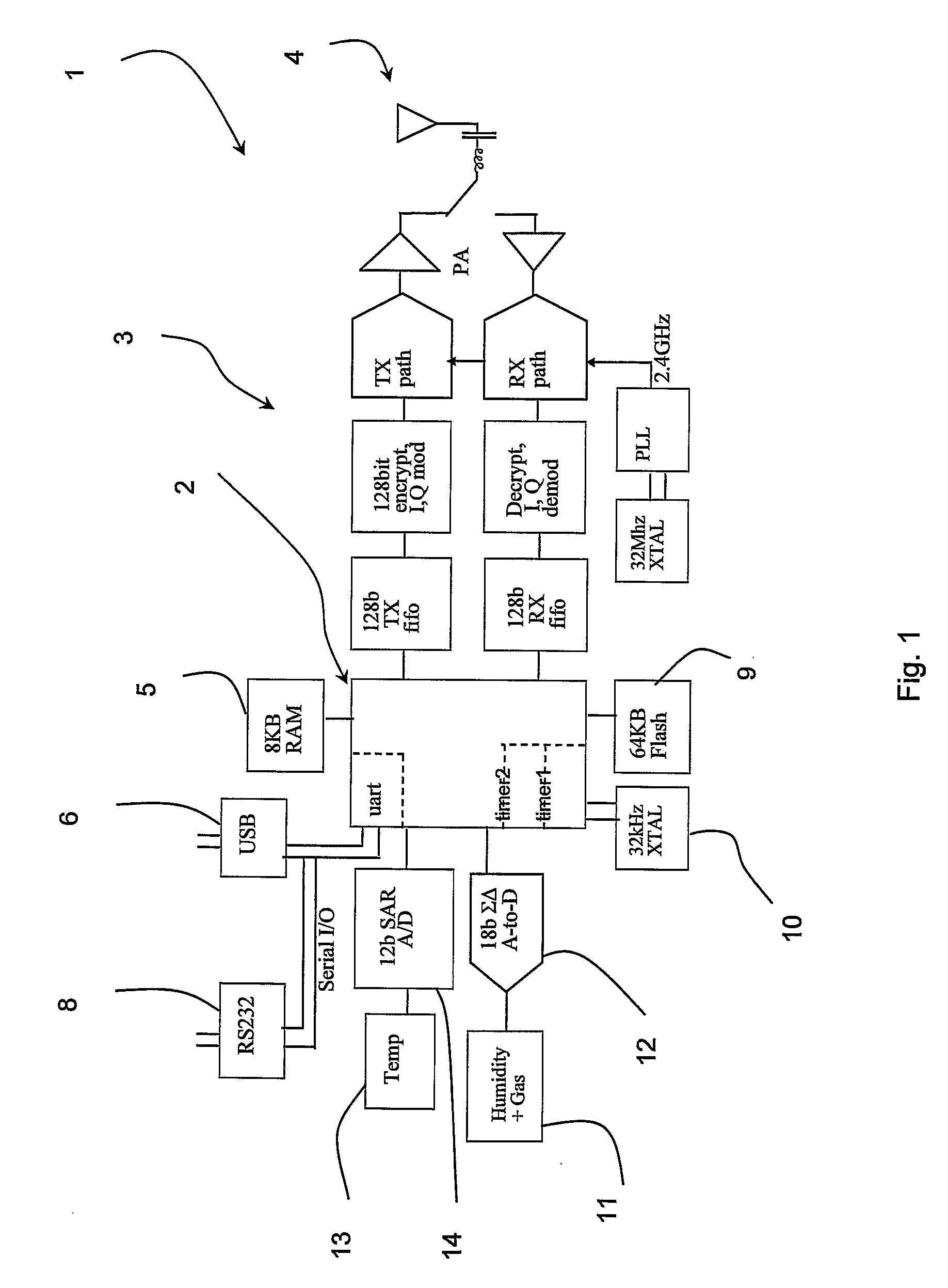
[0050]FIG. 1 is a block diagram of an integrated sensor chip of the invention;

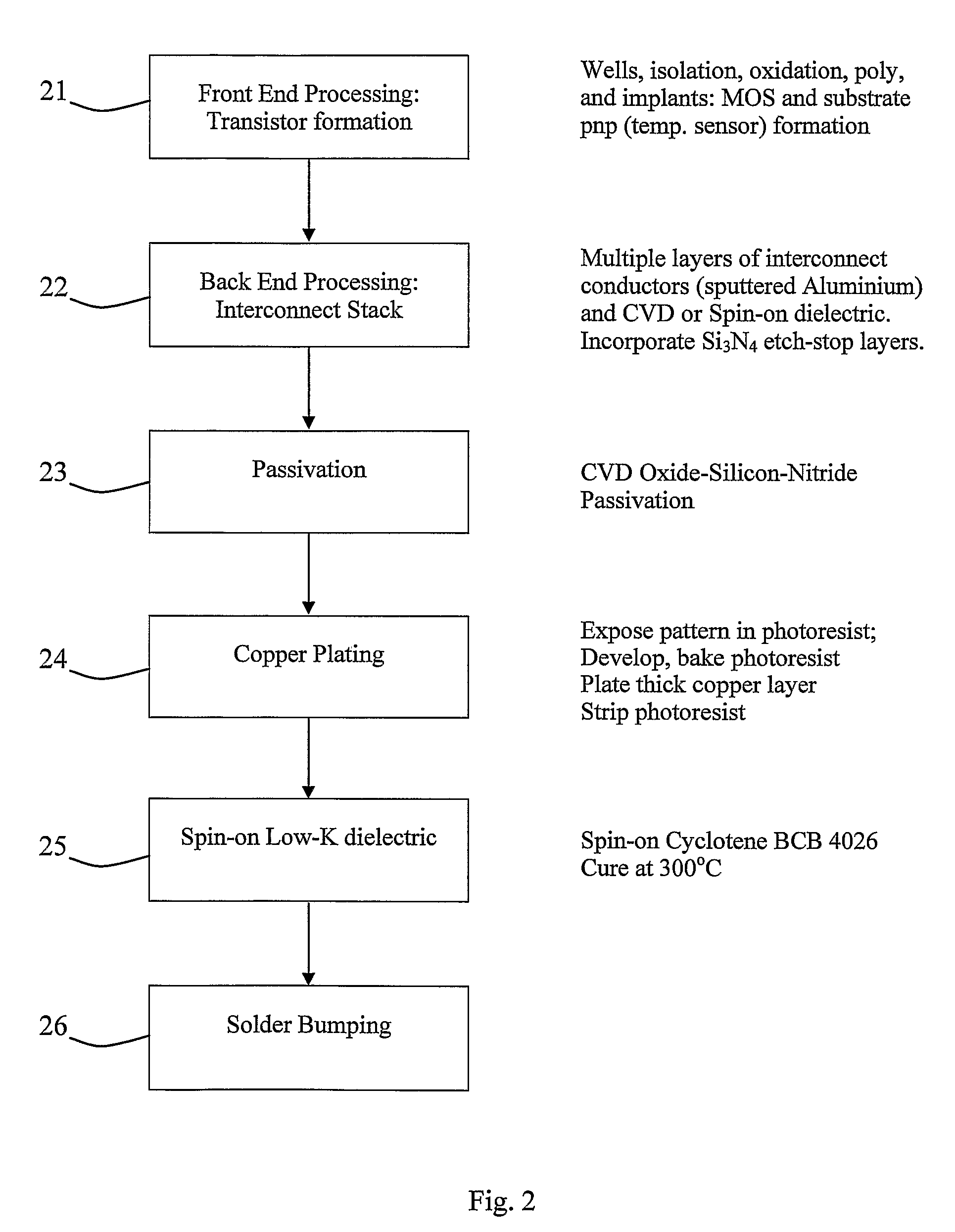
[0051]FIG. 2 is a flow diagram illustrating a production method for the chip;

[0052]FIG. 3 is a diagrammatic cross-sectional representation of the sensor chip together with some plan views of parts of the chip;

[0053]FIG. 4 is a circuit diagram of an 18-bit A-to-D converter of the chip;

[0054]FIGS. 5 to 8 are cross-sectional views of sensing parts of alternative sensor chips of the invention;

[0055]FIG. 9 is a diagram showing chip encapsulation;

[0056]FIG. 10 is a plan view and a diagrammatic side view showing an RFID tag incorporating the chip of the invention;

[0057]FIGS. 11 and 12 are perspective views of probes incorporating chip sensors of the invention;

[0058]FIG. 13 is a circuit diagr...


PUM

PropertyMeasurementUnit
dielectric constantaaaaaaaaaa
temperatureaaaaaaaaaa

Abstract

A single chip wireless sensor (1) comprises a microcontroller (2) connected to a transmit/receive interface (3), which is coupled to a wireless antenna (4) by an L-C matching circuit. The sensor (1) senses gas or humidity and temperature. The device (1) is an integrated chip manufactured in a single process in which both the electronics and sensor components are manufactured using standard CMOS processing techniques, applied to achieve both electronic and sensing components in an integrated process. A Low-K material (57) with an organic polymer component is spun onto the wafer to form a top layer incorporating also sensing electrodes (60). This material is cured at 300° C., which is much lower than CVD temperatures. The polyimide when cured becomes thermoset, and the lower mass-to-volume ratio resulting in K, its dielectric constant, reducing to 2.9. The thermoset dielectric, while not regarded as porous in the conventional sense, has sufficient free space volume to admit enough gas or humidity for sensing.

Description

FIELD OF THE INVENTION[0001]The invention relates to electronic sensors.PRIOR ART DISCUSSION[0002]One of the main driving forces in the electronics industry is the desire to achieve greater integration of finctionality so that production is more automated, and size and per-unit cost reduced. Most importantly, for battery applications, higher integration generally results in lower power, due to reduced parasitic capacitances.[0003]However the continual shrinking of CMOS transistors means that gate delays are reducing, so that overall delays are now becoming dominated by interconnect delay, especially due to the resistivity of Aluminium and capacitance of silicon dioxide (SiO2, dielectric constant K=4 approx). In the field of sensors, and in particular wireless sensors, greater integration has been slow because of the difficulties encountered in integration of microcontroller, A-to-D converter (ADC), EEPROM memory, RF transceiver, and sensor elements in the one integrated sensor devic...

Claims


Application Information

Patent Timeline
Patent Type & Authority Applications(United States)
IPC IPC(8): G01K1/00G01N7/00H01L21/02G01N27/22
CPCG01N27/223
Inventor CUMMINS, TIMOTHY
Owner SILICON LAB INC
Why Eureka
Try Eureka