Method for film depositing group iii nitride such as gallium nitride

Inactive Publication Date: 2009-07-02
SEKISUI CHEM CO LTD
View PDF6 Cites 3 Cited by
  • Summary
  • Abstract
  • Description
  • Claims
  • Application Information

AI Technical Summary

Benefits of technology

[0039]According to the present invention, a group III nitride such as GaN can be grown on a substrate of sapphire or the like using nitrogen plasma in the vicinity of atmospheric pressure. The V/III ratio can be set sufficiently large and the reaction rate can be increased. The substrate temperature can be set lower compared

Problems solved by technology

This makes it difficult to use Si and a high molecular material as a sub

Method used


Image

  • Method for film depositing group iii nitride such as gallium nitride
  • Method for film depositing group iii nitride such as gallium nitride
  • Method for film depositing group iii nitride such as gallium nitride

Examples


embodiment 1

[0145]One embodiment will now be described. It should be noted, however, that the present invention is not limited to this embodiment.

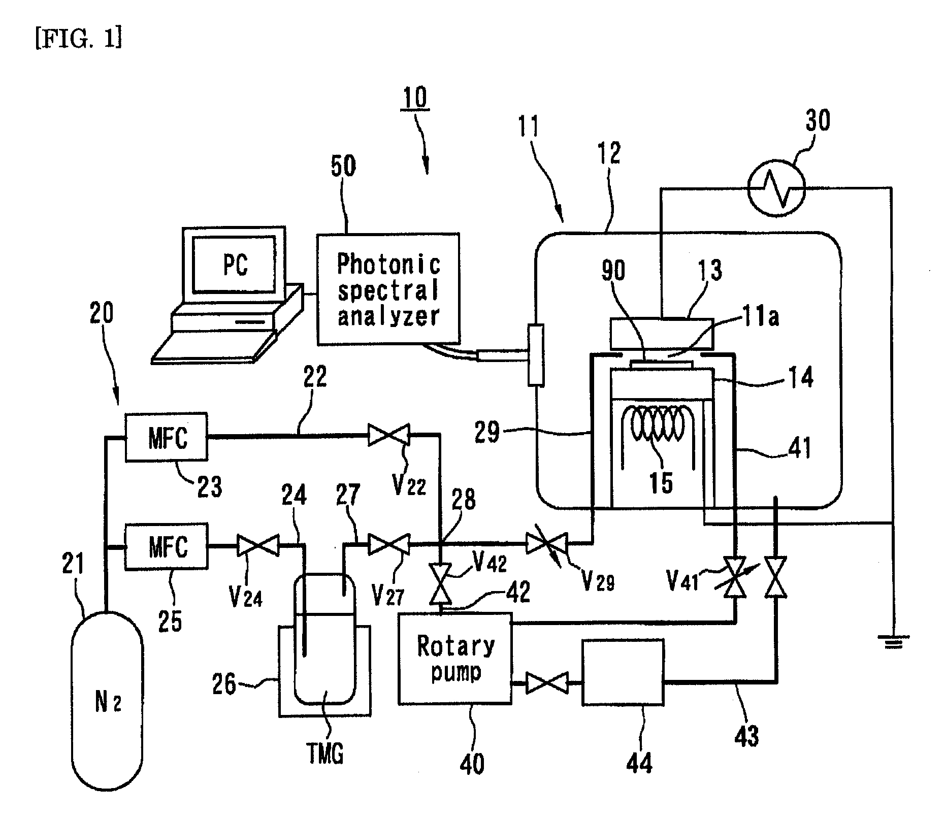
[0146]A film deposition processing was carried out under the following conditions, using the apparatus 10 of FIG. 1.

[0147]N2 flow rate of N2 feed path 22: 300 sccm

[0148]N2 flow rate of carrier feed path 24: 1 sccm

[0149]substrate: c-face sapphire

[0150]substrate temperature: 650 degree centigrade

[0151]processing pressure: 40 kPa

[0152]voltage mode: bipolar pulse wave

[0153]charging voltage: Vpp=500 V

[0154]frequency: 30 kHz

[0155]growth time: 30 min

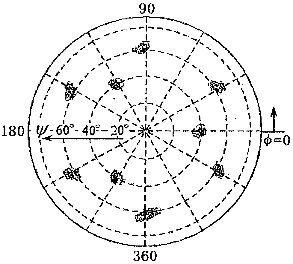
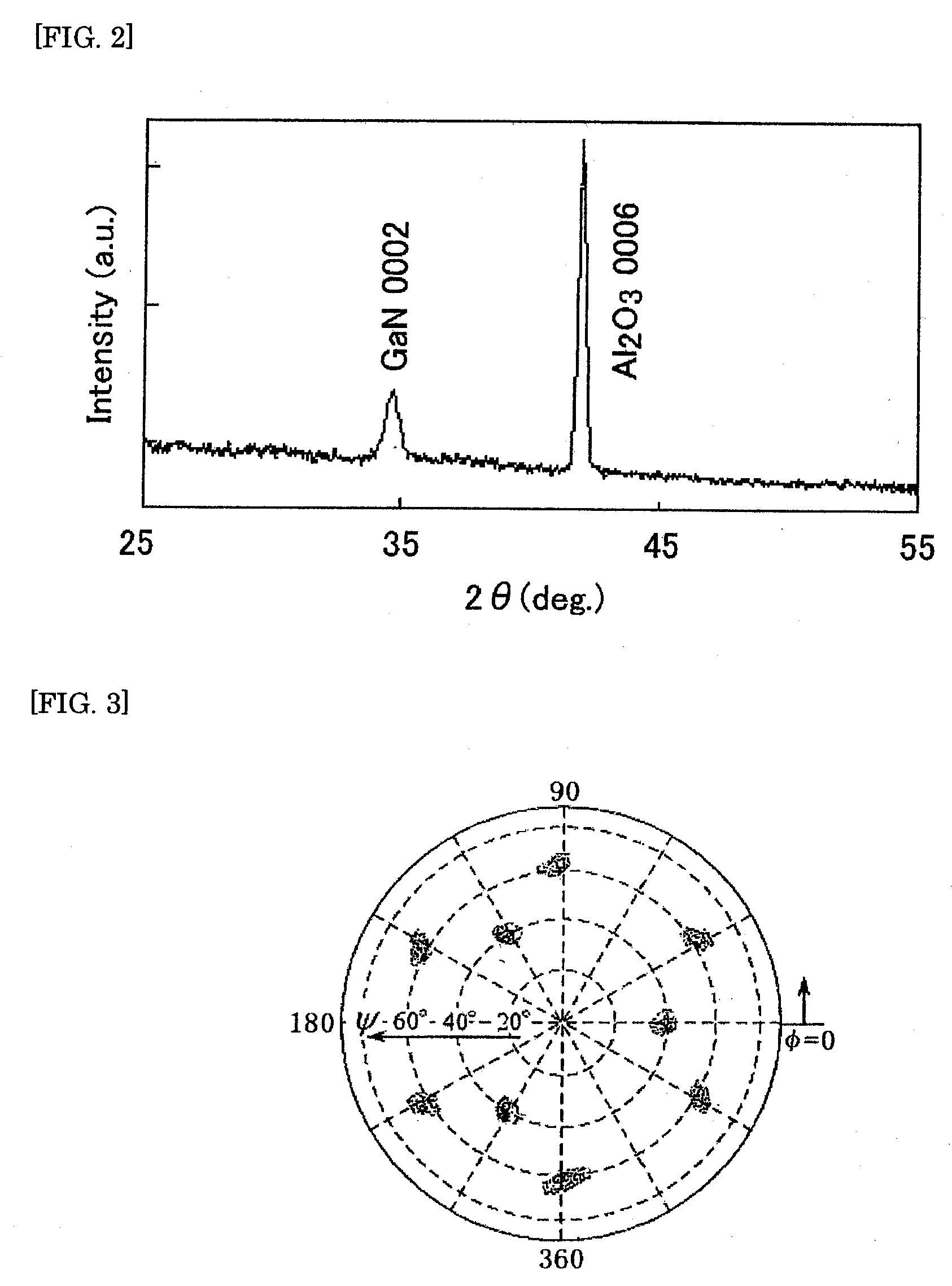
[0156]A sample obtained by the processing of this Embodiment 1 was ω-2θ scan analyzed according to the X-ray diffraction method. As a result, diffraction from the 0002 plane of GaN was confirmed as shown in FIG. 2. Also, the above-mentioned sample was analyzed according to the pole figure method. As a result, 6-times symmetry attributable to a hexagonal structure of the GaN single crystal was confirmed. From the ...

reference experiment 1-1

[0157]In the apparatus 10 of FIG. 1, optical emission from the interelectrode space 11a was analyzed by a photonic spectral analyzer 50. The substrate temperature (Tsub) was set to 650 degree centigrade and only nitrogen was fed into the interelectrode space 11a. As a result, a peak attributable to the 2nd positive system of nitrogen appeared as shown in FIG. 4 and generation of nitrogen plasma was confirmed. It was confirmed that since the plasma is an atmospheric pressure plasma, a main peak appears in a 2nd positive region equal to or less than 337 nm on the higher energy side than in the case of pressure-reduced plasma (414 nm=2.997 eV).

[0158]An insertion Figure encircled with a frame of broken lines in FIG. 4 is an enlargement of a portion covering the wavelength ranging from 350 nm to 400 nm. A peak (390 nm) of ion species, which causes damage to film, was not confirmed.

reference experiment 1-2

[0159]Optical emission from the interelectrode space 11a was analyzed under the following conditions, using a separate photonic spectral analyzer.

[0160]processing pressure (nitrogen atmospheric pressure): 40 kPa plusminus 2 kPa

[0161]feeding gas: only nitrogen, 400 sccm

[0162]substrate temperature: room temperature

[0163]The result is shown in FIG. 5. As shown left down on an enlarged scale, a peak did not appear at the wavelength 391 nm corresponding to the nitrogen ion and nitrogen ion was not confirmed. On the other hand, as shown right down on an enlarged scale, a peak appeared at the wavelength 822 nm corresponding to nitrogen radical and the presence of nitrogen radical was confirmed.


PUM

PropertyMeasurementUnit
Pressureaaaaaaaaaa
Pressureaaaaaaaaaa
Angleaaaaaaaaaa

Abstract

[Problem to be Solved] To film deposit a group III nitride such as GaN using atmospheric pressure plasma.
[Solving Means] A reactor chamber 12 is filled with a pure nitrogen of approximately atmospheric pressure of about 40 kPa. A c-face sapphire substrate 90 is placed on an electrode 14. The substrate temperature is brought to 650 degree centigrade by a heater 15. An electric field is applied between electrodes 13, 14 to form a discharge space 11a therebetween. In a gas feed system 20, a small quantity of trimethylgallium is added to N2, the resultant is fed into a discharge space 11a and brought into contact with the sapphire substrate 90. A V/III ratio on the substrate 90 is brought into a range of from 10 to 100000.

Description

TECHNICAL FIELD[0001]This invention relates to a method for film depositing a group III nitride, such as gallium nitride (GaN), aluminium gallium nitride (AlGaN), aluminium nitride (AlN) or indium nitride (InN) on a substrate.BACKGROUND TECHNIQUE[0002]A group III nitride semiconductor, such as GaN, AlGaN, AlN or InN is expected to be applied not only to an optical emission element but also to a high frequency element. Conventional examples of the method for film depositing a group III nitride are listed below.[0003]1) MOCVD utilizing ammonia[0004]2) MBE utilizing high vacuum plasma[0005]3) MBE under high vacuum utilizing ammonia[0006]4) MOCVD utilizing high vacuum plasma[0007]5) laser abrasion under ultrahigh vacuumPatent Document 1: Japanese Patent Application Laid-Open No. H10-106958Patent Document 2: Japanese Patent Application Laid-Open No. H04-164859Non-Patent Document 1: Development / Application Trend of Compound Semiconductor, Electronic Material (2004) p 18-41[0008]Non-Patent...

Claims


Application Information

Patent Timeline
IPC IPC(8): H01L21/20
CPCC23C16/303C23C16/509C23C16/52C30B25/105H01L21/0262H01L21/0237H01L21/0242H01L21/0254C30B29/403C23C16/34C23C16/50
Inventor NAGATA, TAKAHIROCHIKYO, TOYOHIROUEHARA, TSUYOSHI
Owner SEKISUI CHEM CO LTD
Why Eureka
Try Eureka