Method for manufacturing soi substrate

a technology of silicononinsulator and substrate, which is applied in the direction of basic electric elements, electrical apparatus, semiconductor devices, etc., can solve the problems of insufficient bonding strength between a semiconductor substrate and a base substrate, limited heat treatment temperature, and insufficient treatment, so as to achieve sufficient bonding strength between the semiconductor substrate and the base substra

Inactive Publication Date: 2009-08-13
SEMICON ENERGY LAB CO LTD
View PDF9 Cites 16 Cited by
  • Summary
  • Abstract
  • Description
  • Claims
  • Application Information

AI Technical Summary

Benefits of technology

[0015]By bonding between a semiconductor substrate and a base substrate made from an insulator with an oxide film containing chlorine atoms interposed therebetween, the bonding streng

Problems solved by technology

However, when a substrate having low heat resistance, such as a glass substrate, is used as a base substrate, temperature for heat treatment is more limited (which means that heat treatment needs to be performed through a low-temperature process) than when

Method used


Image

  • Method for manufacturing soi substrate
  • Method for manufacturing soi substrate
  • Method for manufacturing soi substrate

Examples


embodiment mode 1

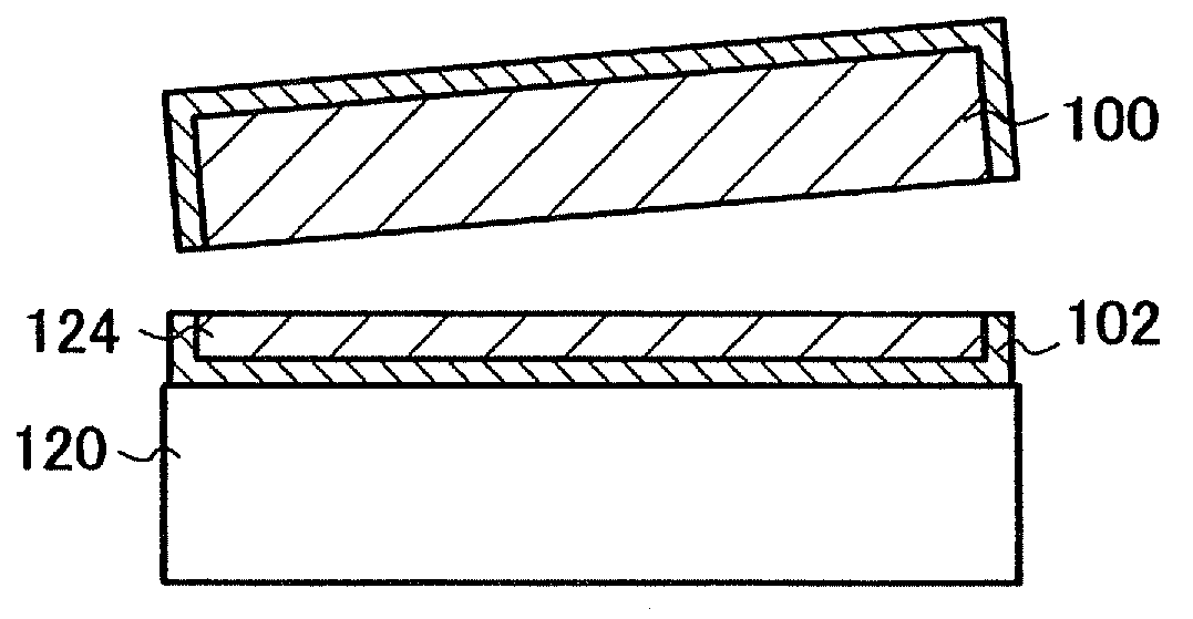
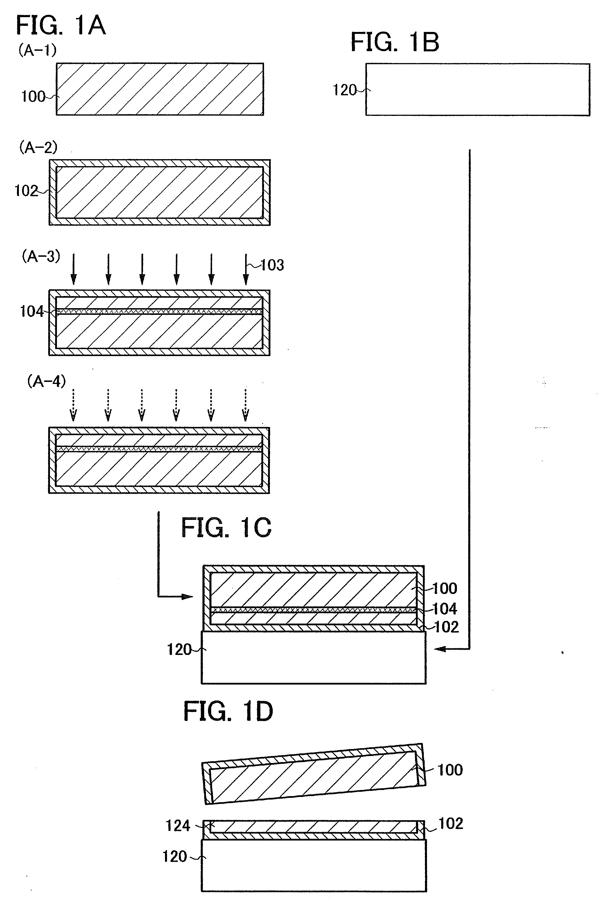
[0029]In this embodiment mode, a method for manufacturing an SOI substrate by bonding a semiconductor substrate and a base substrate is described with reference to drawings.

[0030]First, a semiconductor substrate 100 is prepared (see FIG. 1A-1).

[0031]As the semiconductor substrate 100, a single crystal semiconductor substrate or a polycrystalline semiconductor substrate can be used, and examples thereof include single crystal and polycrystalline silicon substrates, single crystal and polycrystalline germanium substrates, compound semiconductor substrates of gallium arsenide, indium phosphide, and the like. Typical examples of commercially available silicon substrates are circular silicon substrates which are 5 inches (125 mm) in diameter, 6 inches (150 mm) in diameter, 8 inches (200 mm) in diameter, 12 inches (300 mm) in diameter, and 16 inches (400 mm) in diameter. Note that the shape is not limited to a circular shape, and a silicon substrate processed into a rectangular shape or t...

embodiment mode 2

[0081]In this embodiment mode, a method for manufacturing an SOI substrate, which is different from that in the above embodiment mode, is described with reference to drawings. Specifically, a case is described in which an insulating film is formed over a surface of a base substrate.

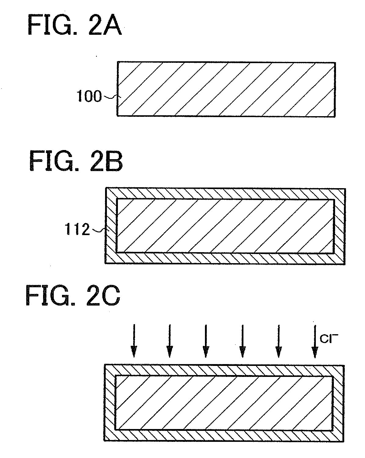
[0082]First, an oxide film 102 is formed over a semiconductor substrate 100; an embrittled region 104 is formed by ion beam irradiation; then, a surface of the oxide film 102 is subjected to oxygen plasma treatment (see FIGS. 3A-1 to 3A-4). Note that, for a specific manufacturing process in FIGS. 3A-1 to 3A-4, the method illustrated in FIGS. 1A-1 to 1A-4 may be referred to; thus, detailed explanation thereof is omitted.

[0083]Next, a base substrate 120 is prepared (see FIG. 3B-1). Then, a semiconductor film 121 is formed over the base substrate 120 (see FIG. 3B-2) and subjected to thermal oxidation treatment in an oxidizing atmosphere containing dichloroethylene to form an oxide film 122 containing chlorin...

embodiment mode 3

[0095]In this embodiment mode, a method for manufacturing a semiconductor device using the SOI substrate manufactured in either one of the above-described embodiment modes is described.

[0096]First, a method for manufacturing an n-channel thin film transistor and a p-channel thin film transistor is described with reference to FIGS. 4A to 4D and FIGS. 5A to 5C. By combining a plurality of thin film transistors (TFTs), various types of semiconductor devices can be formed.

[0097]A case is described in which the SOI substrate manufactured by the method in Embodiment Mode 1 is used as an SOI substrate. It is needless to say that the SOI substrate manufactured by the method in Embodiment Mode 2 can also be used.

[0098]FIG. 4A is a cross-sectional view of the SOI substrate manufactured by the method described with reference to FIGS. 1A-1 to 1A-4, 1B, 1C, and 1D.

[0099]By element isolation of the single crystal semiconductor film 124 by etching, semiconductor films 251 and 252 are formed as ill...


PUM


Abstract

A semiconductor substrate and a base substrate made from an insulator are prepared; an oxide film containing a chlorine atom is formed over the semiconductor substrate; the semiconductor substrate is irradiated with accelerated ions through the oxide film to form an embrittled region at a predetermined depth from a surface of the semiconductor substrate; plasma treatment of the oxide film is performed by applying a bias voltage; a surface of the semiconductor substrate and a surface of the base substrate are disposed opposite to each other to bond a surface of the oxide film and the surface of the base substrate to each other; and heat treatment is performed to cause separation along the embrittled region after bonding the surface of the oxide film and the surface of the base substrate to each other, thereby forming a semiconductor film over the base substrate with the oxide film interposed therebetween.

Description

BACKGROUND OF THE INVENTION[0001]1. Field of the Invention[0002]The present invention relates to a method for manufacturing a silicon-on-insulator (SOI) substrate and a method for manufacturing a semiconductor device.[0003]2. Description of the Related Art[0004]In recent years, integrated circuits have been developed which use a silicon-on-insulator (SOI) substrate in which a thin single crystal semiconductor film is present over an insulating surface, instead of a bulk silicon wafer. The use of an SOI substrate can reduce parasitic capacitance between a drain of a transistor and a substrate; thus, SOI substrates are attracting attention for their ability to improve performance of semiconductor integrated circuits.[0005]One of known methods for manufacturing SOI substrates is a hydrogen ion implantation separation method (for example, see Reference 1: Japanese Published Patent Application No. 2000-124092). A summary of a method for manufacturing an SOI substrate by a hydrogen ion im...

Claims


Application Information

Patent Timeline
IPC IPC(8): H01L21/762
CPCH01L21/76254H01L29/66772H01L27/1266H01L27/1214
Inventor OHNUMA, HIDETOYAMAZAKI, SHUNPEI
Owner SEMICON ENERGY LAB CO LTD
Why Eureka
Try Eureka