

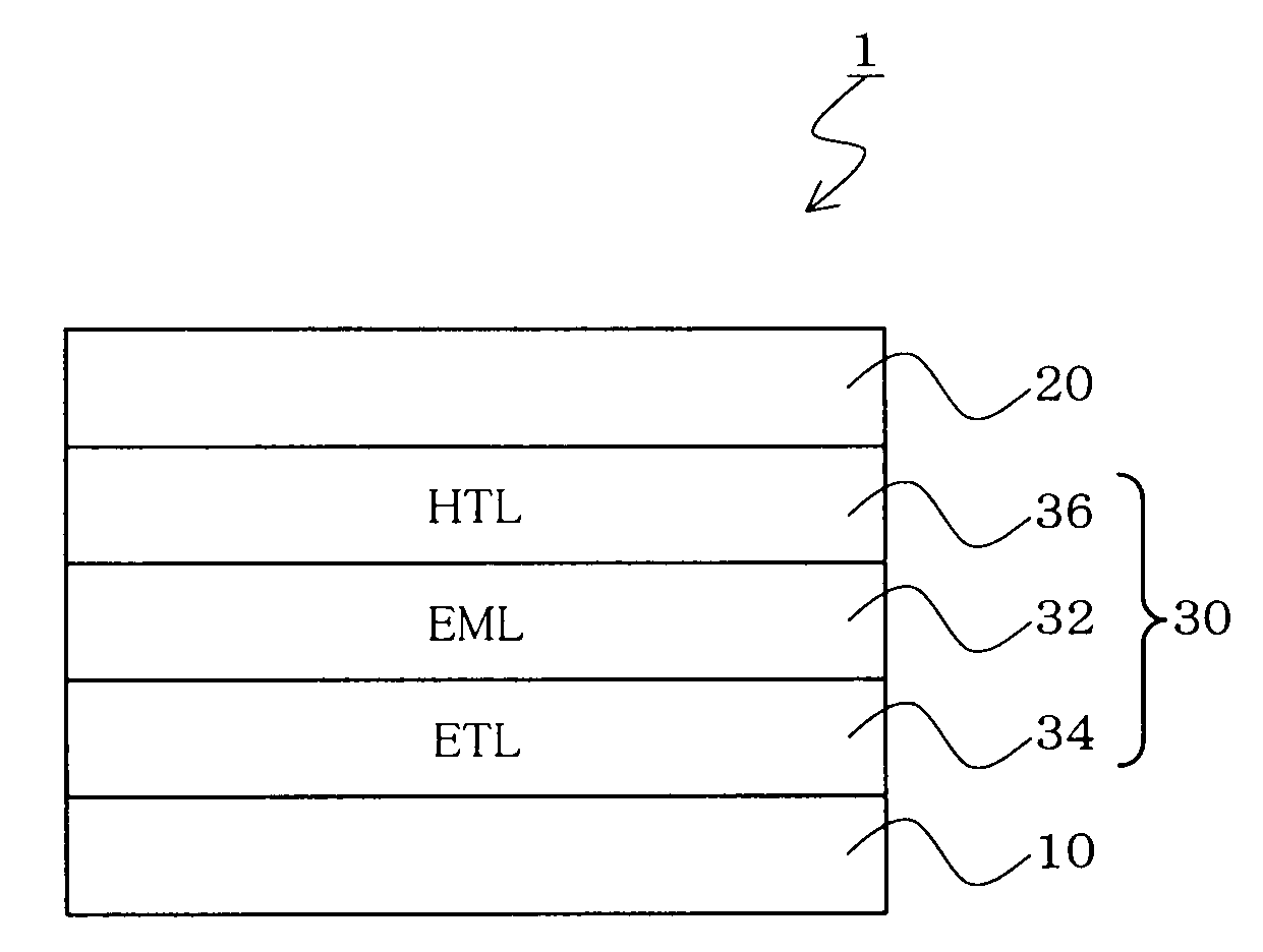
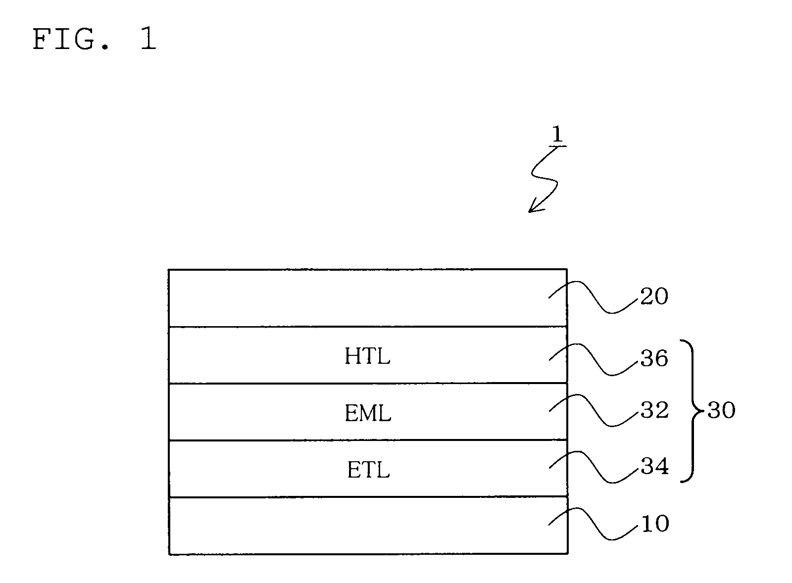
Organic electroluminescence device
a technology of electroluminescence and organs, which is applied in the direction of discharge tubes/lamp details, discharge tubes luminescnet screens, electric discharge lamps, etc., can solve the problems of increasing the driving voltage of the device, unable to obtain durable devices, and ill-balanced devices, etc., to achieve low energy loss from the emitting layer to the electron-transporting layer, and high efficiency and long-lived
- Summary
- Abstract
- Description
- Claims
- Application Information
AI Technical Summary
Benefits of technology
Problems solved by technology
Method used
Image

Examples
example 1
Fabrication of an Organic EL Device
[0177]A glass substrate of 25 mm by 75 mm by 1.1 mm thick with an ITO transparent electrode (GEOMATEC CO., LTD.) was subjected to ultrasonic cleaning with isopropyl alcohol for 5 minutes, and cleaned with ultraviolet rays and ozone for 30 minutes. The thus cleaned substrate with transparent electrode lines was mounted on a substrate holder in a vacuum deposition device. First, a TCTA film was formed in a thickness of 95 nm so as to cover the surface of the transparent electrode on which the transparent electrode lines were formed. This TCTA film functioned as a hole-transporting layer. Subsequent to the formation of the hole-transporting layer, the host A and the complex A were co-deposited in a film thickness of 30 nm by resistance heating. The concentration of the complex A was 7.5 wt %. This host A: complex A film functioned as an emitting layer. Subsequent to the formation of the emitting layer, the electron-transporting material A was formed i...
example 2
[0179]An organic EL device was fabricated and evaluated in the same manner as in Example 1, except that the material B was used as the host material. The results are shown in Table 3.
PUM
 Abstract
Description
Claims
Application Information