[0004]The
rapid acquisition and analysis of high volumes of data in biological samples had its advent in the early days of the human
genome sequencing project.
Microarray technology has facilitated the interrogation of large numbers of samples for biologically relevant patterns in a variety of physiological,
drug-induced or clinically relevant cellular states. A challenge has now presented itself with respect to how these large volumes of information can be integrated into an accurate model of cellular behavior and processes. For example, information relating the effect of a
drug to the extent and duration of
apoptosis in
cancer cells would be invaluable information in a screen for
cancer drugs. Similarly, information of cytoskeletal changes leading to invasiveness would greatly streamline the development of an efficient anti-angiogenic
drug strategy.
[0011]Many protocols for generating data are already well developed in their respective disciplines, from quantitative
Polymerase Chain Reaction (PCR), to
flow cytometry, to
antibody staining. The methods for acquisition of this data, such as different types of optical
microscopy, have already undergone extensive development. Perhaps the most important
image acquisition methods for HCS relate to
cellular imaging, including
drug effect assays for
cytotoxicity,
apoptosis,
cell proliferation, and nucleocytoplasmic transport. Frequently, these approaches utilize cell sensors based on fluorescent proteins and dyes, and thus provide researchers with an ability to screen drugs and to answer more complex biological questions such as target identification and validation and to investigate
gene and
protein function.
[0012]In an effort to fill a need in the art for improved
cellular imaging techniques, the inventors herein disclose a new, inexpensive, and easy-to-use
imaging technology suitable for simultaneous capture of multiple measurements from individual cells that will enable molecular
colocalization,
metabolic state and
motility assessment, and determination of
cell cycle, texture, and morphology. This technology will be capable of not only HCS, but also permit selection of single cells for subsequent high-resolution imaging based on the outputs of the HCS. By increasing the analytical resolution to assess the sub-cellular state
in vivo, the inventors herein hope to increase biological resolution by providing a means to follow the location, timing, and interdependence of biological events within cells in a culture.
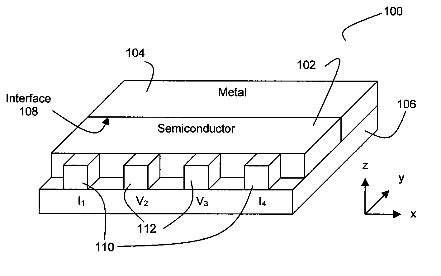
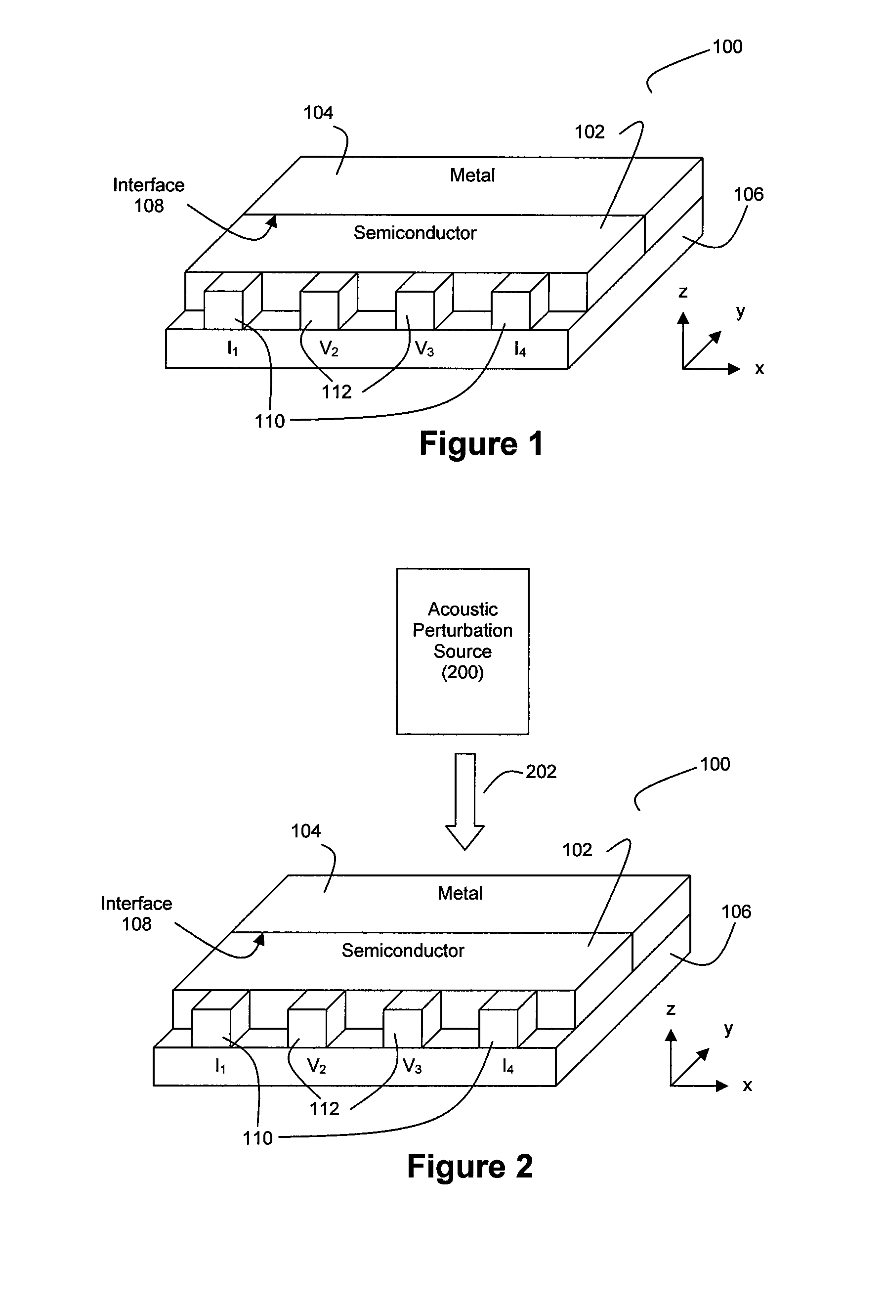
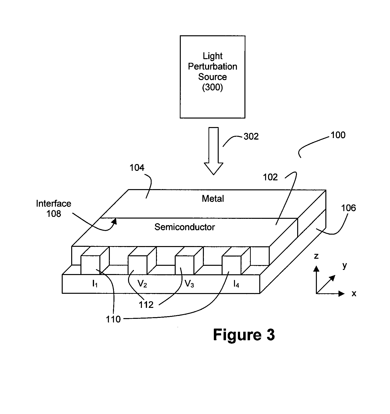
[0015]The inventors herein believe that the use of nanoscale EAC sensors and nanoscale EPC sensors in an
imaging array will provide improved imaging resolution, improved
signal-to-
noise ratio (SNR), and higher bandwidth than conventional ultrasonic or other
modes of detectors. Accordingly, the use of an array having a plurality of nanoscale EAC sensors and / or a plurality of nanoscale EPC sensors can be used for a myriad of applications, including but not limited to
in vitro cell imaging,
in vivo invasive
catheter-based applications for
medical imaging,
endoscopic imaging for gastrointestinal,
prostate, or urethral / bladder / ureteral applications, transdermal
medical imaging for
disease characterization, detection of
abnormal cells in
serum samples, acoustic imaging,
pressure sensing in
nanofluidics, and
blood pressure monitoring inside small vessels.
[0017]The inventors herein further believe that the use of nanoscale EEC sensors in an
imaging array will produce
ultra high resolution images of
electric charge distribution over the surface of one or more living cells, a result that can provide valuable information for monitoring
cancer metastasis and
targeted drug delivery, particularly so when a series of such images are taken over time to track the progression of the cell's
electric charge over time. The inventors herein believe that the nanoscale EEC sensors of the present invention will serve as a significantly more accurate and effective measure of cell electric charge than the conventional
electrophoresis technique that is known in the art because electrophoretic measurements suffer from a complicated instrumental dependence and a lack of spatial resolution.
[0018]The inventors herein further believe that the use of nanoscale EMR sensors in an
imaging array will produce
ultra high resolution images of
magnetoresistance over the surface of one or more living cells, a result that can provide valuable information for studying the magnetic fields produced by nonmagnetic particles embedded in cancer cells, for monitoring magnetically labeled nanoparticles that are trafficking inside the cells or for sensing the evolution of imposed magnetic
resonance spin orientations.


