Field effect transistor, method of manufacturing the same, and semiconductor device

a field effect transistor and semiconductor technology, applied in the direction of semiconductor devices, basic electric elements, electrical appliances, etc., can solve the problems of difficult control of diffusion depth, low threshold voltage uniformity, and positive shift of threshold voltage, so as to reduce the density of traps, reduce the stress generated at the time of temperature reduction after regrowth, and reduce the effect of extraction of ga

Active Publication Date: 2010-01-07
RENESAS ELECTRONICS CORP
View PDF16 Cites 13 Cited by
  • Summary
  • Abstract
  • Description
  • Claims
  • Application Information

AI Technical Summary

Benefits of technology

[0024]A first exemplary aspect of an embodiment of the present invention is a field effect transistor that includes a channel layer of a first conductivity type formed above a semiconductor substrate, an upper semiconductor layer made up of at least one semiconductor layer and formed above the channel layer of the first conductivity type, a semiconductor layer of a second conductivity type formed in a recess made in the upper semiconductor layer or formed above the upper semiconductor layer, a gate electrode formed above and in contact with the semiconductor layer of the second conductivity type, and a gate insulating film including a nitride film formed above and in contact with the upper semiconductor layer and an oxide film formed above the nitride film and having a larger thickness than the nitride film. In this structure, extraction of Ga in the regrowth process is reduced, and it is thereby possible to reduce the density of traps at and near the interface between the gate insulating film and the semiconductor. Further, a stress generated at the time of temperature decrease after regrowth is reduced, and it is thereby possible to suppress the occurrence of crystal defect due to a stress.
[0025]A second exemplary aspect of an embodiment of the present invention is a method of manufacturing a field effect transistor that includes forming a channel layer of a first conductivity type above a semiconductor substrate, forming an upper semiconductor layer containing Ga above the channel layer of the first conductivity type, forming a gate insulating film by forming a nitride film and an oxide film above the upper semiconductor layer containing Ga, selectively regrowing a semiconductor layer of a second conductivity type by using the gate insulating film as a mask, and forming a gate electrode above the semiconductor layer of the second conductivity type. In this method, extraction of Ga in the regrowth process is reduced, and it is thereby possible to reduce the density of traps at and near the interface between the gate insulating film and the semiconductor. Further, residual hydrogen in the nitride film is reduced by heat treatment in the regrowth process, and it is thereby possible to reduce the density of traps occurring by application of high-voltage bias.
[0026]According to the exemplary aspects of an embodiment of the present invention, it is possible to provide a field effect transistor having high reliability with less threshold voltage shift before and after a voltage stress, a method of manufacturing the same and a semiconductor device.

Problems solved by technology

However, in the prior art 1, there is a concern that if a high voltage is applied between the gate and the drain, a positive shift of the threshold voltage is occurred.
However, the nitride film that is deposited by plasma CVD has characteristics that it contains a large amount of residual hydrogen in the film.
Further, the Zn thermal diffusion method used in the prior art 2 has a concern that it is difficult to control a diffusion depth and a threshold voltage uniformity is low.
The increase in the capacitance of the gate parasitic capacitor 42 causes a concern that significant degradation of high-frequency characteristics of an element, such as a decrease in power gain, occurs.
Further, in the prior art 3, because the nitride film 43 with a large film stress is formed at a large thickness, a large stress is generated upon temperature decrease after regrowth, which causes crystal defect or the like.
There is thus a concern that long-term reliability is low.

Method used


Image

  • Field effect transistor, method of manufacturing the same, and semiconductor device
  • Field effect transistor, method of manufacturing the same, and semiconductor device
  • Field effect transistor, method of manufacturing the same, and semiconductor device

Examples


first exemplary embodiment

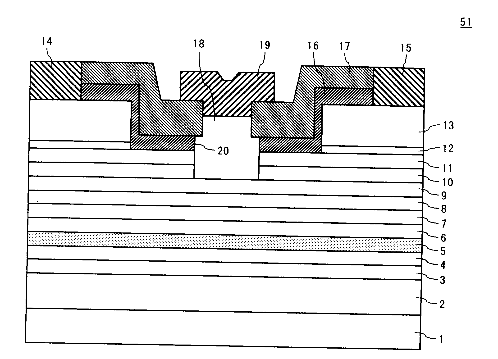
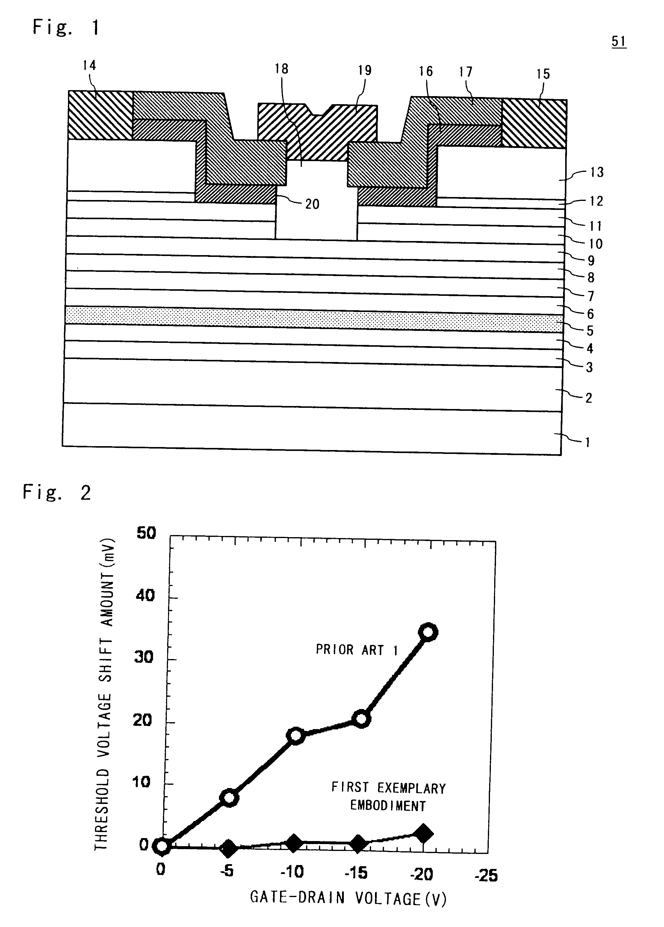
[0055]The structure of a J-FET 51 according to an exemplary embodiment of the present invention is described firstly with reference to FIG. 1. FIG. 1 is a cross-sectional view of the J-FET 51 according to the first exemplary embodiment. Referring to FIG. 1, in the J-FET 51, a buffer layer 2 (with a thickness of 400 nm, for example), a Si-doped n-type AlGaAs electron supply layer 3 (with a thickness of 4 nm, for example), an undoped AlGaAs spacer layer 4 (with a thickness of 2 nm, for example), an undoped InGaAs channel layer 5 (with a thickness of 15 nm, for example), an undoped AlGaAs spacer layer 6 (with a thickness of 2 nm, for example), a Si-doped n-type AlGaAs electron supply layer 7 (with a thickness of 10 nm, for example), an undoped AlGaAs layer 8 (with a thickness of 5 nm, for example), an undoped GaAs layer 9 (with a thickness of 5 nm, for example), an undoped InGaP stopper layer 10 (with a thickness of 5 nm, for example), an undoped GaAs gate burying layer 11 (with a thic...

second exemplary embodiment

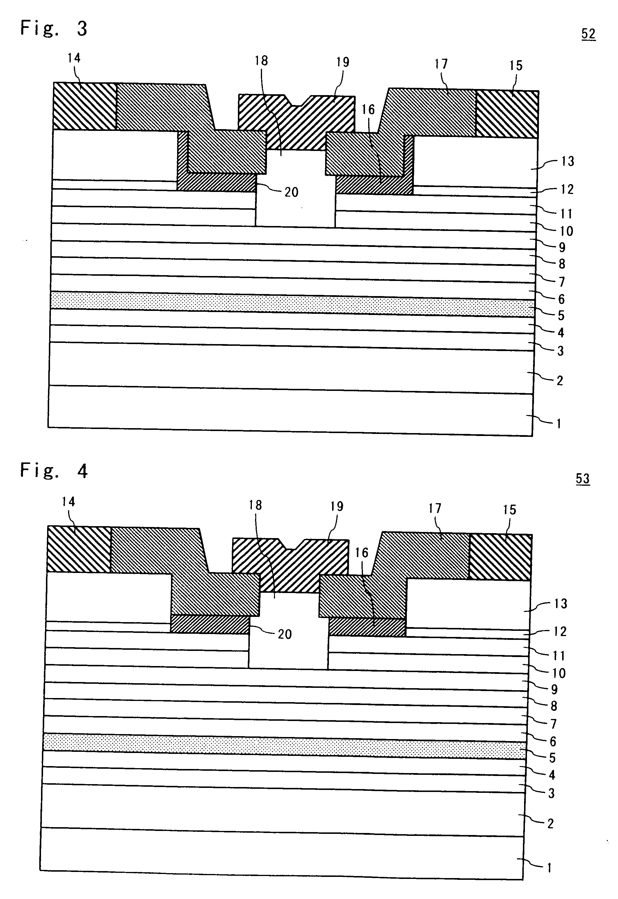
[0075]The structure of a J-FET 54 according to an exemplary embodiment of the present invention is described hereinafter with reference to FIG. 5. FIG. 5 is a cross-sectional view of the J-FET 54 according to a second exemplary embodiment of the present invention. Although the side-etch 20 is formed in the nitride film 16 as shown in FIG. 1 according to the first exemplary embodiment, the side-etch 20 is not formed as shown in FIG. 5 according to this exemplary embodiment. The other structure is the same as that of the first exemplary embodiment and not repeatedly described.

[0076]Referring to FIG. 5, in this exemplary embodiment, the nitride film 16 is not side-etched deeper than the oxide film 17, and the pattern end of the nitride film 16 facing the gate electrode 19 and the pattern end of the oxide film 17 facing the gate electrode 19 are located in the same positions. The J-FET 54 having such a structure is formed by applying dry etching conditions with enhanced anisotropy when ...

third exemplary embodiment

[0077]The structure of a J-FET 55 according to an exemplary embodiment of the present invention is described hereinafter with reference to FIG. 6. FIG. 6 is a cross-sectional view of the J-FET 55 according to a third exemplary embodiment of the present invention.

[0078]As shown in FIG. 6, in this exemplary embodiment, a Si-doped n-type InGaP stopper layer 21 to which a Si impurity is added at high concentrations is formed instead of the Si-doped n-type AlGaAs stopper layer 12 of the J-FET 51 according to the first exemplary embodiment. The other structure is the same as that of the first exemplary embodiment and thus not repeatedly descried. Because the InGaP layer has a lower potential barrier for electrons than the AlGaAs layer, contact resistance from the C-doped p+-GaAs layer 18 to the undoped InGaAs channel layer 5 is reduced. Thus, lower on-resistance can be obtained in the J-FET 55 using InGaP compared to the case of using AlGaAs. In such a case also, the same advantages as in...


PUM


Abstract

A J-FET includes a channel layer of a first conductivity type (a Si-doped n-type AlGaAs electron supply layers 3 and 7, undoped AlGaAs spacer layers 4 and 6, and an undoped InGaAs 5 channel layer 5) formed above a semi-insulating GaAs substrate, an upper semiconductor layer made up of at least one semiconductor layer and formed above the channel layer of the first conductivity type, a semiconductor layer of a second conductivity type (C-doped p+-GaAs layer 18) formed in a recess made in the upper semiconductor layer or formed above the upper semiconductor layer, a gate electrode placed above and in contact with the semiconductor layer of the second conductivity type, and a gate insulating film including a nitride film formed above and in contact with the upper semiconductor layer and an oxide film formed above the nitride film and having a larger thickness than the nitride film.

Description

BACKGROUND OF THE INVENTION[0001]1. Field of the Invention[0002]The present invention relates to a field effect transistor, a method of manufacturing the same and a semiconductor device and, particularly, to a p-n junction gate field effect transistor using a p-type semiconductor layer as a gate.[0003]2. Description of Related Art[0004]A junction field effect transistor (J-FET) using a p-type semiconductor layer as a gate has a higher gate forward turn-on voltage than a GaAs field effect transistor having a Schottky gate electrode. Thus, a J-FET has a feature that it can highly bias a gate voltage positively and has a high maximum drain current (Imax). Particularly, a J-FET in which a p-type semiconductor layer is formed only just under the gate electrode by using selective regrowth technology has better in-wafer uniformity of a threshold voltage than a J-FET having a p-n junction gate formed by a thermal diffusion method, and it is known as a promising device structure (e.g. cf. Ja...

Claims


Application Information

Patent Timeline
Patent Type & Authority Applications(United States)
IPC IPC(8): H01L29/812H01L21/338
CPCH01L21/8252H01L29/7785H01L27/0605
Inventor BITO, YASUNORI
Owner RENESAS ELECTRONICS CORP
Why Eureka
Try Eureka