Excepting switching transients, the ID·VDS product in the
power MOSFET remains small, and power dissipation in the switch remains low.
Unfortunately the Schottky has several major disadvantages, the one of which is that it exhibits significant and unwanted off-state leakage current, especially at high temperatures.
Unfortunately there is a fundamental tradeoff between a Schottky's off-state leakage and its forward-biased
voltage drop.
Moreover, this leakage exhibits a positive
voltage coefficient of current, so that as leakage increases, power dissipation also increases causing the Schottky to leak more and dissipate more power causing even more heating.
With such
positive feedback, localized heating can cause a hot spot to get hotter and “hog” more of the leakage till the spot reaches such a
high current density that the device fails, a process known as
thermal runaway.
Another
disadvantage of a Schottky is the difficulty of integrating it into an IC using conventional
wafer fabrication processes and manufacturing.
Commonly available metals exhibit too high of a voltage barrier, i.e. too high a
voltage drop.
Conversely, other commonly available metals exhibit too low of a barrier potential, i.e. suffer from too much leakage.
The
synchronous rectifier MOSFET however, unlike the Schottky or junction
diode, allows current to flow bi-directionally and must be operated with precise timing on its gate
signal to prevent
reverse current flow, unwanted conduction which lowers efficiency, increase power dissipation and heating, and may damage the device.
Isolated
converters require transformers that are too large compared to single-winding inductors and suffer from unwanted stray inductances.
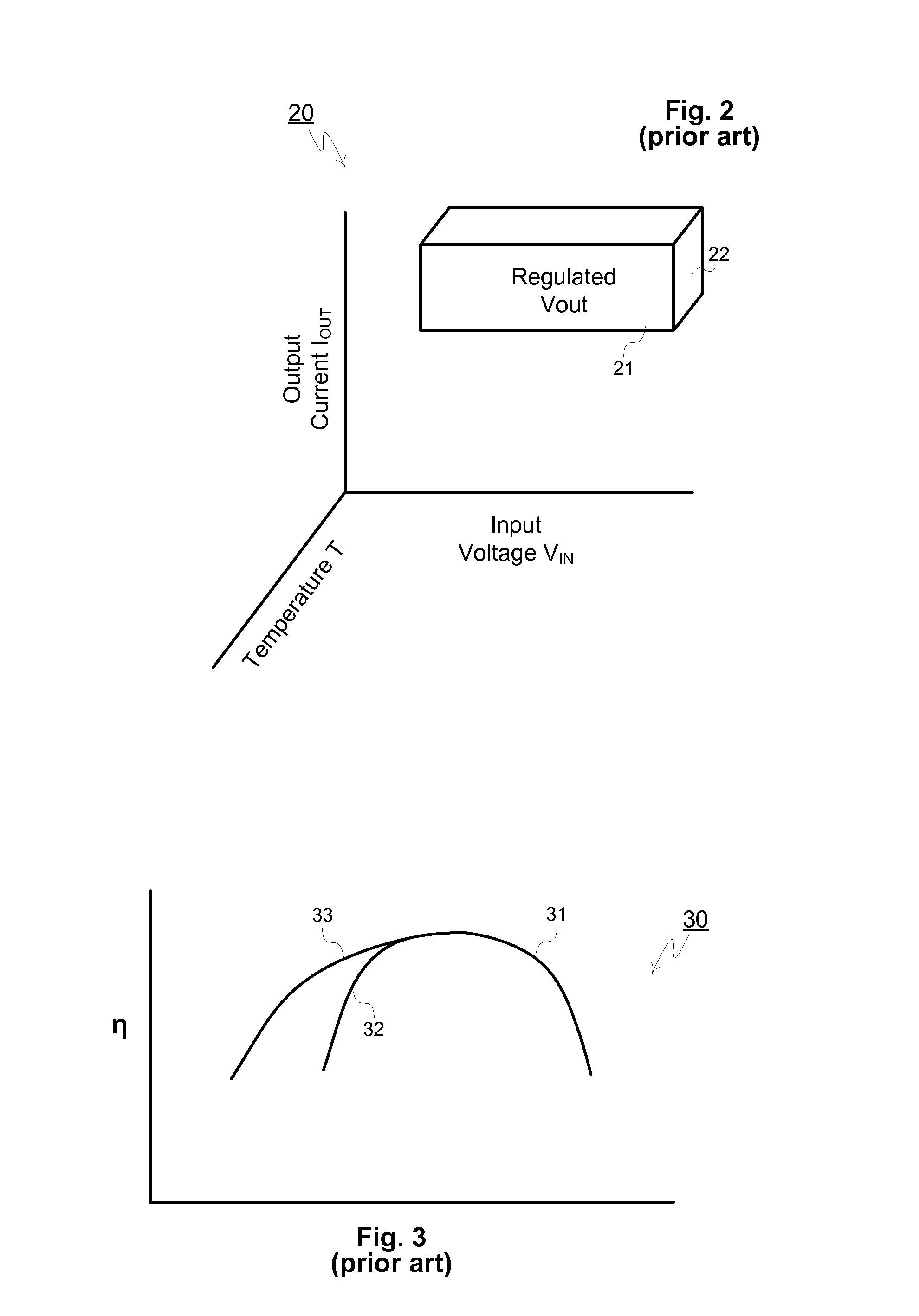
Maintaining high efficiency over the entire range of the “box” is difficult especially for voltage regulators subjected to wide variations in load current or input voltage.
For example, it may be difficult to achieve efficient operation at
high load currents when VIN is low because the power-MOSFETs have inadequate gate drive to turn-on fully, i.e. with a low source-
drain resistance.
Over-
sizing the MOSFETs for
low input voltage conditions may cause excessive switching losses when the input voltage is high.
Prior art techniques of varying the frequency or the conducting time of the power MOSFETs to extend the high efficiency range 33 have been developed and are well known but limited in their benefit.
The efficiency challenge is exacerbated by the fact that during in
general purpose operation dramatic changes in load current can occur at any time and with no warning, so that the
regulator must be prepared to react to the changes at all times even if they occur infrequently.
If the
regulator cannot react quickly enough, the output voltage will exhibit a spike up or down outside the specified tolerance range of the regulator, potentially resulting in
system malfunction or damage to other electronic components.
The problems imposed by operating the switching regulator at different output voltages are many.
First the optimization of the regulator's design for one output voltage may differ dramatically for another voltage, affecting efficiency, transient regulation, and even stability.
For example, a regulator working well for a 2.5V output may at 3.3V become unstable and oscillate, or may not be able to deliver a regulated 1.1V output under any circumstances.
A second problem in changing the output voltage occurs during the dynamic transition during operation, i.e. when the load is subjected to a changing voltage.
During the transition, the converter may become unstable or lose regulation temporarily.
so that higher gate drive voltage results in lower resistance and lower conduction losses.
Specifically, at low voltages switching losses are dominated by
gate capacitance driving losses Pdrive.
Higher gate voltages therefore increases gate drive losses.
Since higher gate drive reduces conduction losses, an unavoidable tradeoff exists between
conduction loss and gate drive loss.
but still exhibits the same gate drive loss.
So in a synchronous converter the gate drive losses are always occurring in both MOSFETs all the time.
But since RDS is inversely proportional to gate width that method results in increased conduction losses.
Unfortunately in conventional power MOSFETs once the gate width is chosen and the device is design in the
integrated circuit, it cannot be changed.
If the current suddenly increases while a small gate width MOSFET is being used, during the
finite time it takes to measure the current and dynamically adjust the MOSFET's size, the output voltage will drop and unacceptably poor regulation will result.
Existing switching regulators are not able to adaptively maximum their efficiency relative to changing currents.
In normal applications however, voltage current and temperature vary naturally and their influence on converter efficiency cannot be avoided.
But even operating within this
restricted range of conditions, significant performance compromises exist.
Other design parameters which appear to be within the power supply circuit designer's control in fact are not, either because it is impractical to do so or because it may adversely affect other electrical circuitry in the
system being regulated.
For example, during normal full load current operation, varying the
switching frequency f of a converter is generally considered unacceptable, especially in communication devices such as
cell phones, because it produces a varying and unpredictable
noise spectrum, difficult to filter or suppress.
Optimizing gate drive is also problematic.
Moreover the input voltage varies over time so the efficiency will unavoidably vary with the input.
For example in a battery powered application the input voltage may be too high in voltage for optimum operation when the battery input is in its fully charged condition, leading to unwanted and excessive capacitive gate drive losses.
When the battery is nearly discharged, the voltage may be inadequate to achieve full channel conduction in the MOSFET leading to
high resistance and excessive conduction losses.
While this premise is true in theory, in practice a dynamic regulation problem results.
The practical drawback of this technique is substantial and has essentially prevented the successful commercialization and any practical use of the technique.
Because the switching device is unnecessarily large, a temporarily condition occurs exhibiting lower
overall efficiency.
The loss of efficiency occurs because the gate drive losses remain fixed in absolute power, but the delivered power to the load drops, so that the gate drive loss increases on a percentage basis lowering the converter's
overall efficiency.
So using the variable gate width technique, a decrease in load current does not cause any problem in accurately maintaining a regulated voltage, just a momentary period of lower efficiency.
In the other case, i.e. a step-function increase in load current, serious performance deficiencies can occur.
Specifically if the load current increases dramatically and without warning, the prior-art variable-gate-width switching regulator may not have time to react, the voltage falls outside the specified range, and regulation is lost.
But because the MOSFET's gate width has been reduced to a small W during the prior condition, its resistance is too high to rapidly increase the inductor's current.
Even if in the next cycle the MOSFET's gate width is increased, it may be too late to increase the inductor's current sufficiently to avoid a voltage transient from occurring on the regulator's output.
In fact, the converter may require many cycles before it finally adjusts the MOSFET to an adequate size to carry the necessary current to react to the load transient.
In extreme cases, the degradation in regulation accuracy may in fact render the converter unusable.
In other words, the prior-art variable-width switching regulator is incapable of regulating a
constant voltage over a range of load currents because it cannot react quickly enough to maintain regulation.
Prior art attempts to vary the gate width in response to changing load currents in a fixed-output voltage switching
voltage regulator resulted in poor or unacceptable
voltage regulation of load transients.
Similarly, using the prior art techniques to optimize efficiency in a switching regulator with a variable output suffer the same regulation issues as fixed output regulators.
In either case, the converter does not have adequate time to react to changing load currents and regulation suffers.
So while the converter's
slow response results in poor transient regulation, the unpredictability of the load current is the condition that causes the problem.
In conclusion, today's varying the gate width of the power MOSFETs in a switching regulator helps reduce switching losses and widen the range of currents with conversion efficiency but at the expense of suffering poor regulation.
As a result such wide-efficiency converters have not been commercially successful.
Biased at low currents, a
comparator suffers slow slew rates, op amps exhibit low bandwidths, and the converter needs time to respond to any significant change in the load or input condition.
Dynamically changing switching frequencies to control switching losses creates
noise spectra almost impossible to filter out of sensitive communication circuitry.
Even worse, new applications demand that the output voltage of a switching regulator be dynamically programmable in real time under the control of a
microprocessor, digital controller, or
baseband processor.
In every aforementioned prior art method attempting to widen the range of a switching regulator's efficiency, especially for
light load operation, the converter's poor regulation is a problem of reaction time.
A switching regulator operating to save power takes a long time to sense and react to changes, especially changes in load current.
But part of the problem lies in the belief that load current is unpredictable, that it must be sensed to know what it is.
The load current sensing and transient regulation problem only worsens if the output voltage is also allowed to vary dynamically too.

