

Light emitting device using gan led chip
- Summary
- Abstract
- Description
- Claims
- Application Information
AI Technical Summary
Benefits of technology
Problems solved by technology
Method used
Image

Examples
embodiment 1
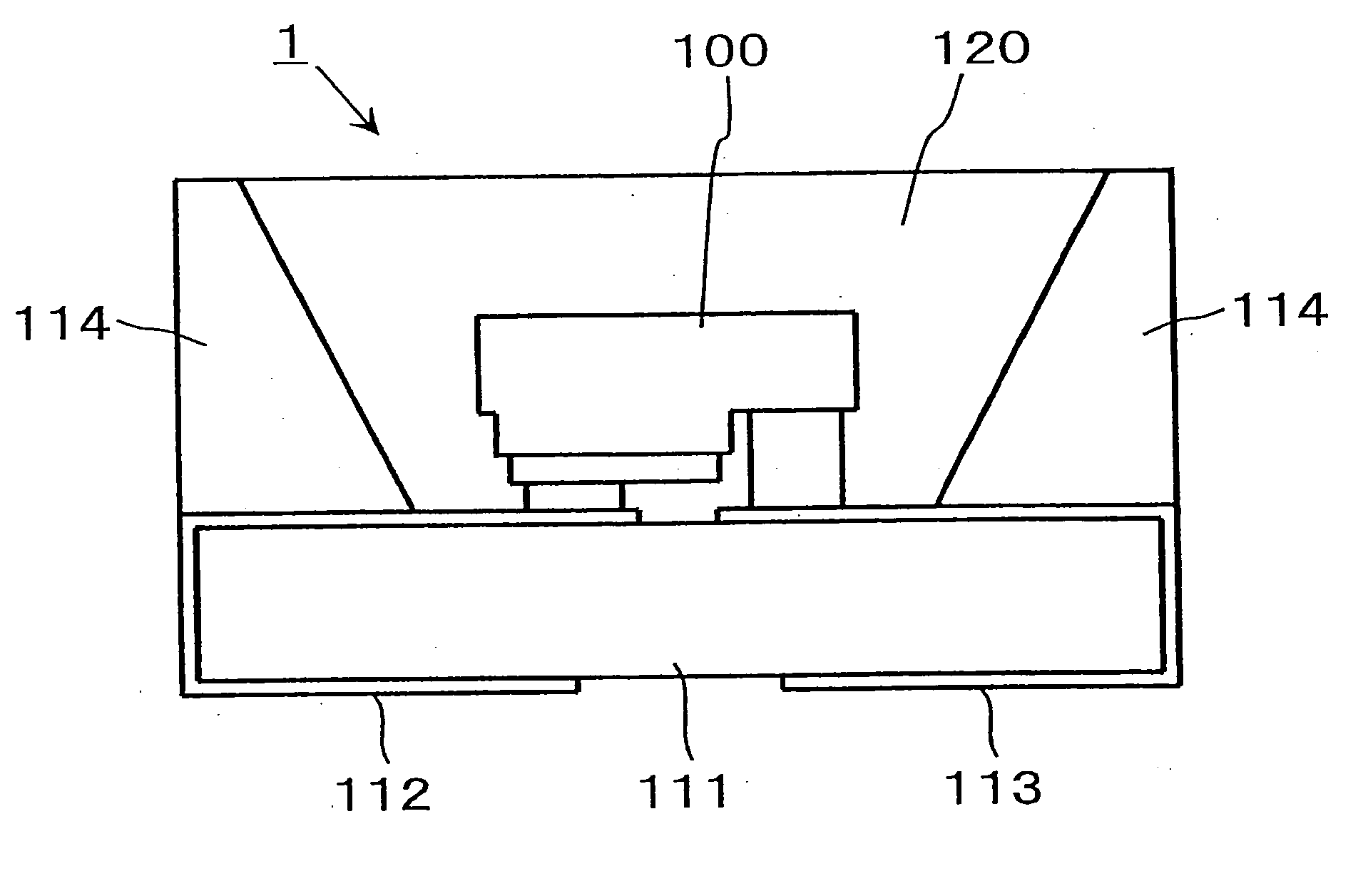
[0049]FIG. 1 is a sectional view of a light emitting device according to an embodiment of the present invention. The light emitting device 1 shown in this Figure exhibits a form of SMD (Surface Mount Device)-type LED package, and a GaN-based LED chip 100 of the above-mentioned (a) is flip-chip mounted on a substrate 111 made of ceramic, resin and the like. The GaN-based LED chip 100 is fixed by bonding each of the positive electrode and negative electrode formed on the same side of the LED chip 100 to electrodes 112 and 113 formed on the substrate 111. As a bonding agent (not shown), one having electrical conductivity, for example, a solder such as Au—Sn solder, a conductive paste such as silver paste and the like, is used. A reflector 114 is, in this embodiment, an independent part from the substrate 111, though it can also be integrally formed with the substrate. A light-transmissive encapsulant 120 such as an epoxy resin and a silicone resin fills a cavity (cup-shaped part) const...
embodiment 2
[0065]FIG. 3 is a sectional view of a light emitting device according to another embodiment of the present invention. The light emitting device 2 shown in this Figure is a bullet type LED package, wherein a GaN-based LED chip 200 is flip-chip mounted in a cup-shaped part formed in a lead frame 211 and molded with a light-transmissive encapsulant 220 having a bullet shape. The light-transmissive encapsulant 220 is, for example, an epoxy resin. The GaN-based LED chip 200 is fixed by bonding a positive electrode formed on one side of the LED chip 200 to the lead frame 211. In this embodiment, the GaN-based LED chip 200 has a vertical-type element structure, and a negative electrode is formed on a chip surface opposite the positive electrode. This negative electrode is connected to the lead frame 212 by a bonding wire 213. When a white light emitting device is produced, a phosphor is dispersed in the light-transmissive encapsulant 220. It will be understood from the inclusion of this ex...
experimental example 1
Production of GaN-Based LED Chip
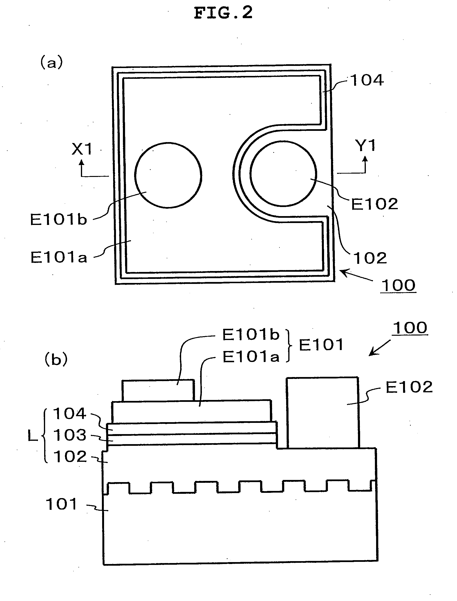
[0083]As a substrate for crystal growth, a c-plane sapphire substrate (diameter 2 inch) processed to have a stripe-like concave-convex pattern (groove width and ridge width: about 3 μm, groove depth: about 1 μm) on the surface was prepared. Using a usual MOVPE apparatus, an LED wafer was produced by successively laminating, on the surface with the above-mentioned concave-convex pattern of the sapphire substrate, an AlGaN low-temperature buffer layer, a non-doped GaN layer, a Si-doped GaN contact layer, an InGaN / GaN multiple quantum well active layer (light emitting layer), a Mg-doped AlGaN clad layer and a Mg-doped AlGaN contact layer. Here, the crystal composition of the InGaN quantum well layer contained in the active layer was adjusted to have an emission wavelength of about 405 nm. Mg added as p-type impurity to the AlGaN clad layer and AlGaN contact layer was activated after formation of the AlGaN contact layer by first introducing a small amount...
PUM
 Abstract
Description
Claims
Application Information