Continuous coating installation, methods for producing crystalline solar cells, and solar cell

a technology of crystalline solar cells and continuous coatings, applied in the direction of pv power plants, sustainable manufacturing/processing, final product manufacturing, etc., can solve the problems of high production rate, low deposition rate of crystalline thin films, and inability to produce high-quality semiconductor structures cost-effectively, so as to avoid the melting of the underlying layer

Inactive Publication Date: 2010-02-04
CARL ZEISS SMT GMBH +1
View PDF13 Cites 73 Cited by
  • Summary
  • Abstract
  • Description
  • Claims
  • Application Information

AI Technical Summary

Benefits of technology

[0021]In principle, it is possible to move the entire laser crystallization system. In order to keep the moved masses small, however, it is often more expedient to move only individual optical components. A particularly advantageous configuration, which is distinguished by its simplicity and extensive minimization of the masses to be moved, provides for a laser beam movement device to have a moveable mirror that deflects the at least one laser beam onto the at least one sub-partial area. A suitable arrangement of this or, if appropriate, the plurality of such deflection mirrors makes it possible to direct the laser beam or laser beams at each desired location on the substrate.
[0048]It can be particularly advantageous for high throughput and low production costs of the continuous coating installation for the laser radiation to be reflected back after reflection at the a-Si or melted Si layer by mirrors onto the same location again in order to increase the power or to reduce the desired laser power under the same process conditions. On account of the high reflectivity of the melted silicon, approximately 50% depending on angle of incidence and wavelength, the efficiency of the installation can be increased by this “beam recycling”.

Problems solved by technology

In general, however, the deposition rates for producing the crystalline thin films are too low to be able to produce high-quality semiconductor structures cost-effectively.
In this case, however, the growth rate is generally only a few tens of nanometres per minute.
Thin films produced by high-rate methods such as, e.g., electron beam evaporation or cathode sputtering generally have an amorphous microstructure and generally are not readily suitable for electronic components.
Thermal crystallization of an amorphous silicon film may not suitable for producing crystalline silicon layers having crystallites of significantly larger than approximately 1 μm.
With the aid of laser processes, although thin films having thicknesses of more than 200 nm can be crystallized, there can be difficulty with process control.

Method used


Image

  • Continuous coating installation, methods for producing crystalline solar cells, and solar cell
  • Continuous coating installation, methods for producing crystalline solar cells, and solar cell
  • Continuous coating installation, methods for producing crystalline solar cells, and solar cell

Examples


first embodiment

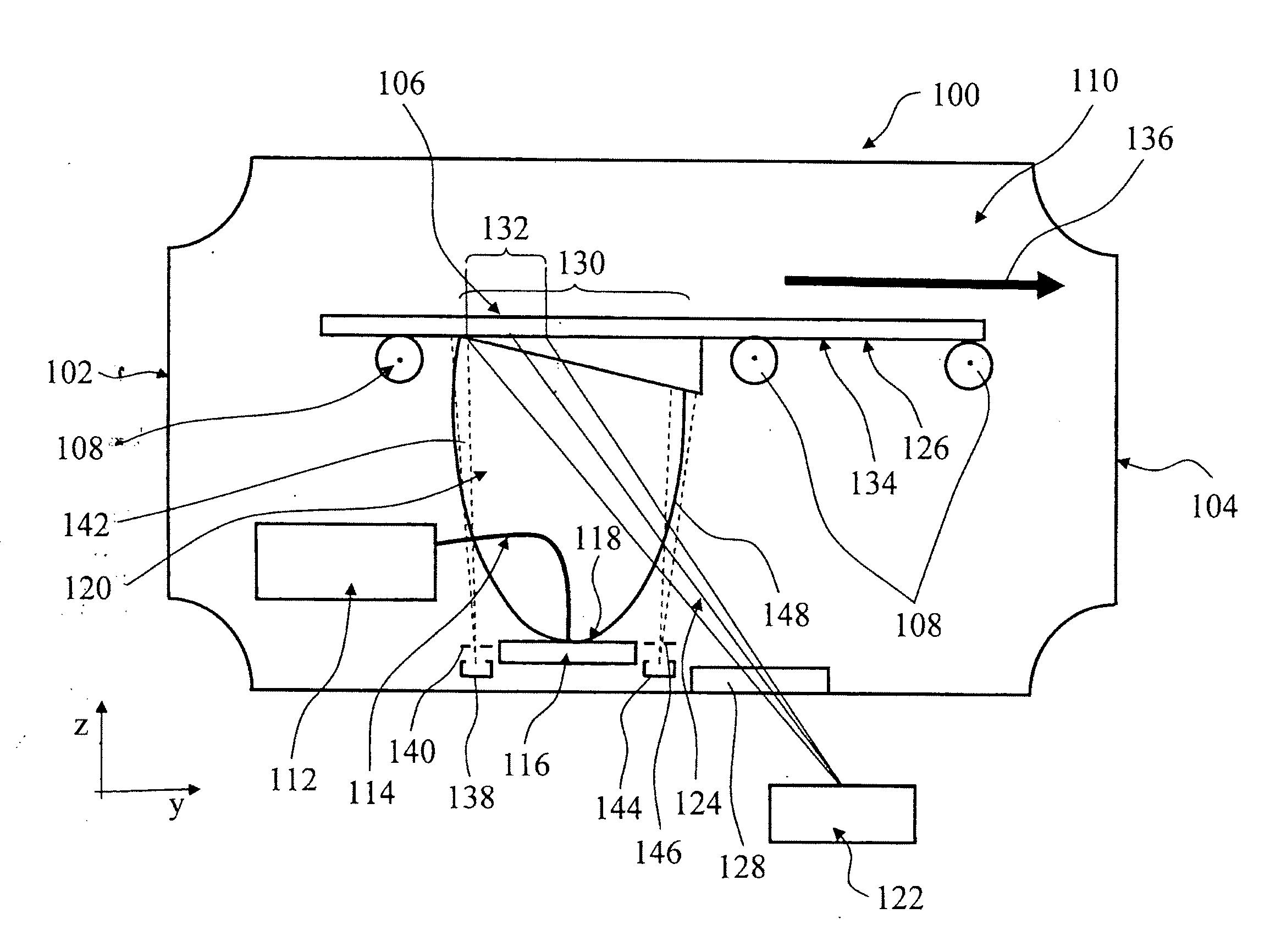
[0078]FIG. 3 shows a coating installation 200 with a first embodiment variant of a laser crystallization system 122. The basic illustration reveals a vacuum chamber 110 with supply and discharge opening 102, 104 and chamber window 128.

[0079]Constituent parts of the installation 200 are, alongside the laser crystallization system 122, a transport device (not illustrated here) and also a PVD coating device (likewise not illustrated) (if appropriate with effusion cell(s)) of the type shown in FIGS. 1 and 2.

[0080]In this embodiment variant according to FIG. 3 , the laser crystallization system 122 includes three lasers 202, 204, 206. The latter emit laser beams 254, 256, 258 having a power of 300 watts, a pulse frequency of 300 hertz and a laser energy of one joule per pulse.

[0081]The laser beams 254, 256, 258 are respectively directed onto two-dimensional single-stage homogenizers 208, 210, 212. The homogenized laser beams 260, 262, 264 emerging from the homogenizers 208, 210, 212 on t...

third embodiment

[0090]FIG. 5 shows a further continuous coating installation 400 with a third embodiment variant of a laser crystallization device 122.

[0091]The continuous coating installation 400 again includes a vacuum chamber 110 with a supply opening 102, via which a substrate 106 can be supplied in feedthrough direction 136, and with a discharge opening 104, via which the substrate 106 can be removed in feedthrough direction 136. A constituent part of the continuous coating installation 400 is once again a PVD coating device (not illustrated), which can be arranged above or below the substrate 106. In this respect, the continuous coating device 400 is identical to that according to FIG. 4.

[0092]A third embodiment variant of a laser crystallization device 122 is depicted as a further constituent part of the continuous coating installation 400 in FIG. 5 of the drawing. As in the previous exemplary embodiment, the laser crystallization device 122 includes three lasers 402, 404, 406 having a power...


PUM

PropertyMeasurementUnit
grain diametersaaaaaaaaaa
thicknessesaaaaaaaaaa

Abstract

A continuous coating installation is disclosed. The installation includes a vacuum chamber having a supply opening for supplying a substrate to be coated and a discharge opening for discharging the coated substrate. The installation also includes a physical vapour deposition device for coating a surface of the substrate, and a laser crystallization system for simultaneously illuminating at least one sub-partial area of a currently coated partial area of the surface of the substrate with at least one laser beam. The installation further includes a transport device for transporting the substrate in a feedthrough direction from the supply opening to the discharge opening and for continuously or discontinuously moving the substrate during the coating thereof in the feedthrough direction.

Description

CROSS-REFERENCE TO RELATED APPLICATIONS[0001]This application is a continuation of, and claims benefit under 35 USC 120 to, international application PCT / EP2008 / 001465, filed Feb. 25, 2008, which claims benefit of U.S. Ser. No. 60 / 903,739, filed Feb. 27, 2007. International application PCT / EP2008 / 001465 is hereby incorporated by reference in its entirety.FIELD[0002]The disclosure relates to a continuous coating installation, such as for producing nano-, micro-, poly-, multi- or monocrystalline thin films, referred to hereinafter generally as crystalline thin films. The disclosure also relates to a method for producing crystalline thin films, such as for producing a silicon tandem solar cell. The disclosure further to a tandem solar cell which can be produced using the methods disclosed herein.BACKGROUND[0003]Semiconductor components used in microelectronics and photovoltaics are predominantly based on the semiconductor material silicon. The single-crystal semiconductor wafers which ...

Claims


Application Information

Patent Timeline
Patent Type & Authority Applications(United States)
IPC IPC(8): H01L31/0376H01L21/20C23C14/34
CPCC23C14/18C23C14/30C23C14/562C23C14/5813H01L31/076H01L31/1824H01L31/1872H01L31/206Y02E10/545Y02E10/548Y02P70/50
Inventor SHAH, ARVINDSCHADE, HORSTMUENZ, HOLGERVOELCKER, MARTINSCHALL, MICHAELKRANTZ, MATTHIAS
Owner CARL ZEISS SMT GMBH
Why Eureka
Try Eureka