

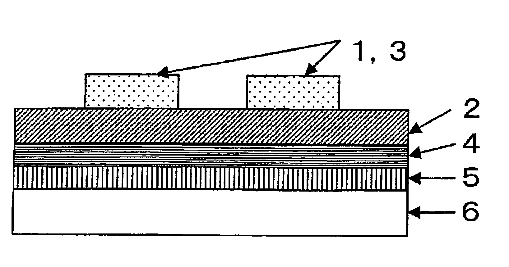
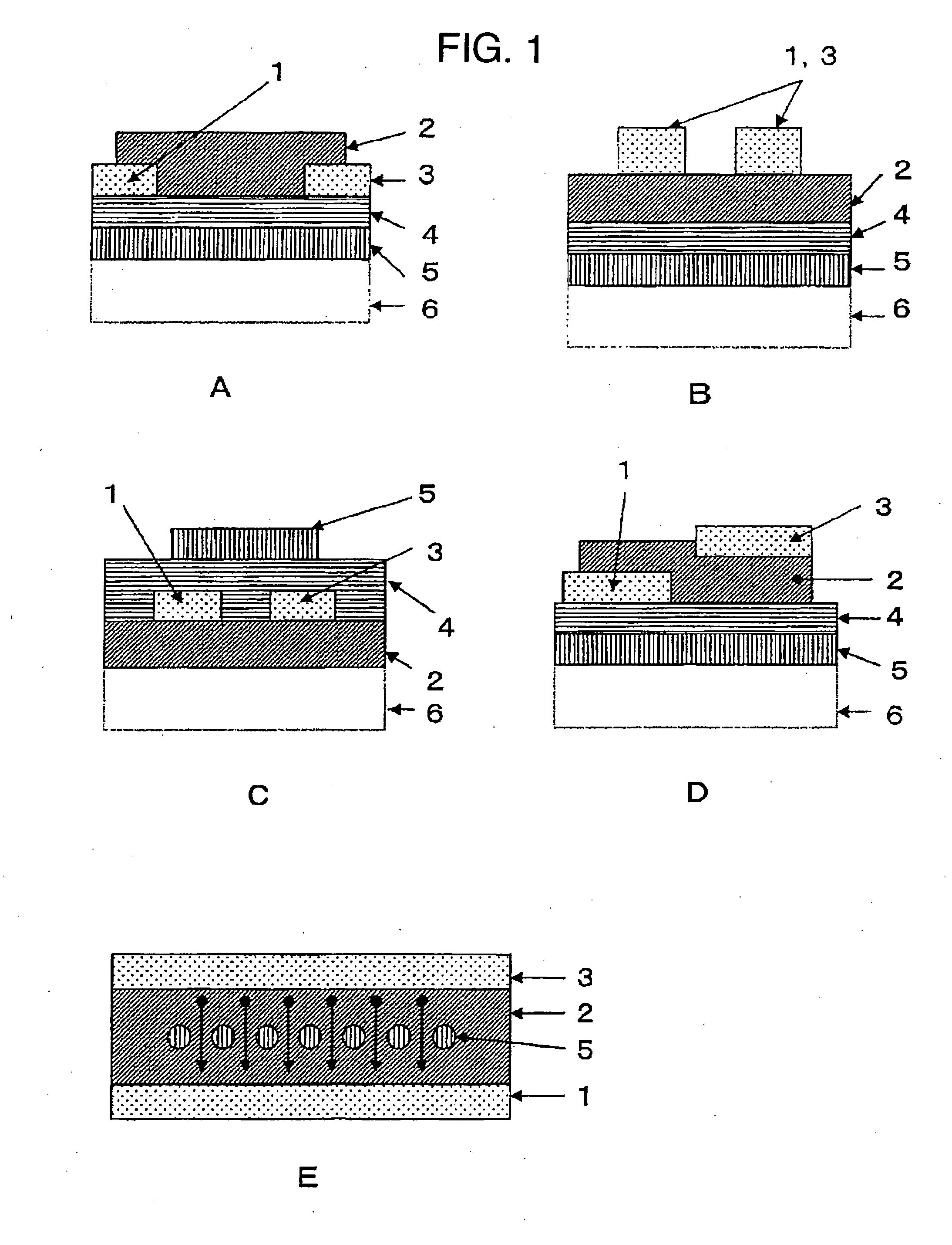
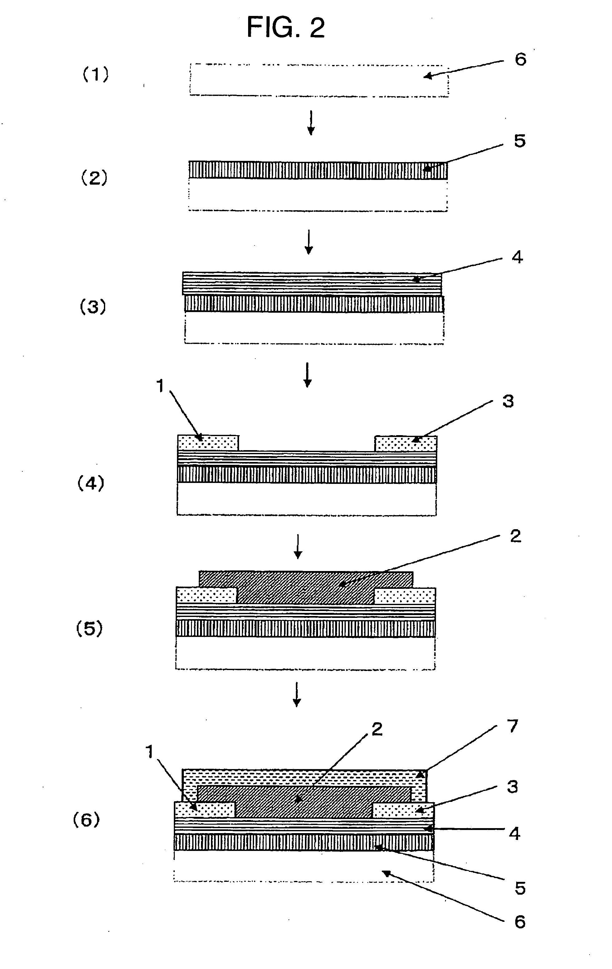
Field-effect transistor
a field-effect transistor and transistor technology, applied in the field of field-effect transistors, can solve the problems of high equipment investment, high cost, and high energy consumption, and achieve the effects of excellent carrier mobility, suitable printing properties, and excellent stability
- Summary
- Abstract
- Description
- Claims
- Application Information
AI Technical Summary
Benefits of technology
Problems solved by technology
Method used
Image

Examples
synthesis example 1
Synthesis of 2,7-Di(1-octynyl)[1]benzothieno[3,2-b][1]benzothiophene
[0126]
[0127]After 2,7-Diiodobenzothienobenzothiophene (1.0 g, 2.0 mmol) was dissolved in anhydrous diisopropylamine (15 ml) and anhydrous benzene (15 ml) under a nitrogen atmosphere, deaeration was performed for 30 minutes. To this, 10 mol % PdCl2 (PPh3)2 (140 mg), 20 mol % CuI (76 mg) and 1-octyn (0.81 ml, 5.5 mmol) were added and stirred at room temperature for 8 hours. After completion of stirring, water (30 ml) was added and extraction was performed with chloroform (30 ml×3). The extraction solution was washed with water (100 ml×3) and dried over anhydrous magnesium sulfate. The solvent was distilled away under reduced pressure and purification was performed by column chromatography (silica gel, methylene chloride: hexane=1:3, Rf=0.6). Recrystallization was performed from hexane to obtain the desired compound in the form of a colorless plate-crystal represented by the formula (5) above (yield: 710 mg, yield coef...
synthesis example 2
Synthesis of 2,7-Dioctyl[1]benzothieno[3,2-b][1]benzothiophene
[0136]
[0137]The compound (300 mg, 0.66 mmol) represented by the formula (5) above and obtained in Synthesis Example 1 and Pd / C (70 mg) were added to anhydrous toluene (10 mL). The reaction mixture was reduced in pressure by an aspirator and purged with hydrogen. This operation was repeated several times and then the reaction mixture was stirred for 8 hours. After completion of the reaction, the solvent was distilled away. Purification was performed by column chromatography (silica gel, hexane, Rf=0.6) (yield: 286 mg, yield coefficient: 94%) and recrystallization was performed from hexane to obtain the desired compound represented by the formula (6) above in the form of colorless powdery solid substance (yield: 250 mg, yield coefficient: 82%). This compound is the compound of Compound No. 16 of Table 1 above.
[0138]1H-NMR (400 MHz, CDCl3):
[0139]δ7.75 (d, J=8.2 Hz, 2H), 7.68 (d, J=1.5 Hz, 2H), 7.26 (dd, J=8.2, 1.5 Hz, 2H), 2...
synthesis example 3
Synthesis of 2,7-Di(1-dodecynyl)[1]benzothieno[3,2-b][1]benzothiophene
[0146]
[0147]The same process as in Synthesis Example 1 was repeated except that 1-dodecyne was used in place of 1-octyne of Synthesis Example 1 to obtain the desired compound represented by the formula (7) above (yield: 966 mg, yield coefficient: 85%). This compound is the compound of Compound No. 91 of Table 1 above.
[0148]1H-NMR (400 MHz, CDCl3):
[0149]δ7.93 (dd, J=1.4, 0.52, 2H), 7.74 (dd, 7=0.52, 8.3 Hz, 2H), 7.45 (d, J=1.4, 8.3 Hz, 2H), 2.44 (t, J=7.1, 4H), 1.59-1.67 (m, 4H), 61.43-1.51 (m, 4H), 1.28-1.32 (m, 24H), 0.88 (t, J=6.8 Hz, 6H)
[0150]13C-NMR (400 MHz, CDCl3):
[0151]142.2, 134.0, 132.0, 128.4, 126.9, 121.2, 121.0, 91.6, 80.4, 31.9, 29.61, 29.56, 29.3, 29.2, 29.0, 28.8, 22.7, 19.5, 14.1
[0152]MS (70 ev, DI) m / z=568 (M+)
[0153]mp 96-97° C.
[0154]Anal. Calcd for C38H48S2: C, 80.22; H, 8.50
[0155]Found: C, 80.12; H, 8.34
PUM
| Property | Measurement | Unit |
|---|---|---|
| temperature | aaaaa | aaaaa |
| thickness | aaaaa | aaaaa |
| thickness | aaaaa | aaaaa |
Abstract
Description
Claims
Application Information