
Method of growing zinc-oxide-based semiconductor and method of manufacturing semiconductor light emitting device

a technology of zinc oxide and light-emitting devices, which is applied in the direction of single crystal growth, polycrystalline material growth, chemistry apparatus and processes, etc., can solve the problems of low productivity, low defect density, and low defect density, and achieve excellent single crystal quality and low defect density. , the effect of high performan

Inactive Publication Date: 2010-03-18
STANLEY ELECTRIC CO LTD
View PDF5 Cites 6 Cited by
  • Summary
  • Abstract
  • Description
  • Claims
  • Application Information

AI Technical Summary

Benefits of technology

[0011]The present invention was made in view of the above-described problems, and objects thereof are to provide a method of growing a zinc-oxide-based semiconductor crystal which has a small number of crystal defects or low defect density and is excellent in single-crystal quality and flatness over a substrate, and to provide high performance, high reliability semiconductor devices, especially high performance semiconductor light emitting devices excellent in light-emission efficiency and device lifetime, and in addition to provide semiconductor light emitting devices high in production yield and excellent in mass productivity.

Problems solved by technology

The MBE method is a crystal growth method performed under an ultrahigh vacuum, and hence there is the problem that the apparatus for it is expensive and that productivity is low.
However, the method disclosed in Reference 1 is a growth condition / method effective only for the MBE method and cannot be applied to the MOCVD method.
However, with these methods, when the polycrystal is single-crystallized by heat treatment, defects are left between adjacent crystal grain boundaries, and when the actual buffer layer is grown from the micro crystals with grains merging, defects are left.
Hence, it is difficult to greatly reduce the number of crystal defects.
As such, to date, attempts to improve crystallinity after forming a buffer layer of a polycrystal, micro crystals, or amorphous material have been made, but the method to improve crystallinity for the MOCVD method is complex, and it has been difficult to grow a ZnO-based crystal of high crystalline quality on a substrate.
As described above, methods of growing a ZnO-based single crystal on a sapphire substrate or the like using the MOCVD method have been proposed in large number, but they fall short of being a method of growing a ZnO-based single crystal of high crystalline quality in a simple, convenient way.
With this polycrystal or imperfect single crystal strongly oriented in a crystal axis direction, grain boundaries and dislocations cause a leak current or local current concentration in semiconductor devices, resulting in degradation of device characteristics and device lifetime.
In particular, in semiconductor light emitting devices, leak currents and current concentration result in degradation of characteristics such as light-emission efficiency and device lifetime.
Further, the crystal surface being not even or flat results in a decrease in process accuracy in semiconductor processes such as lithography and etching and a decrease in production yield, and also results in a decrease in production yield in cleavage, breaking, and the like.
As such, to date, it has been difficult to grow a ZnO-based semiconductor single crystal which is flat and has a small number of grain boundaries and dislocations, on a substrate of another material such as a sapphire substrate by the MOCVD method.

Method used


Image

  • Method of growing zinc-oxide-based semiconductor and method of manufacturing semiconductor light emitting device
  • Method of growing zinc-oxide-based semiconductor and method of manufacturing semiconductor light emitting device
  • Method of growing zinc-oxide-based semiconductor and method of manufacturing semiconductor light emitting device

Examples


embodiment 1

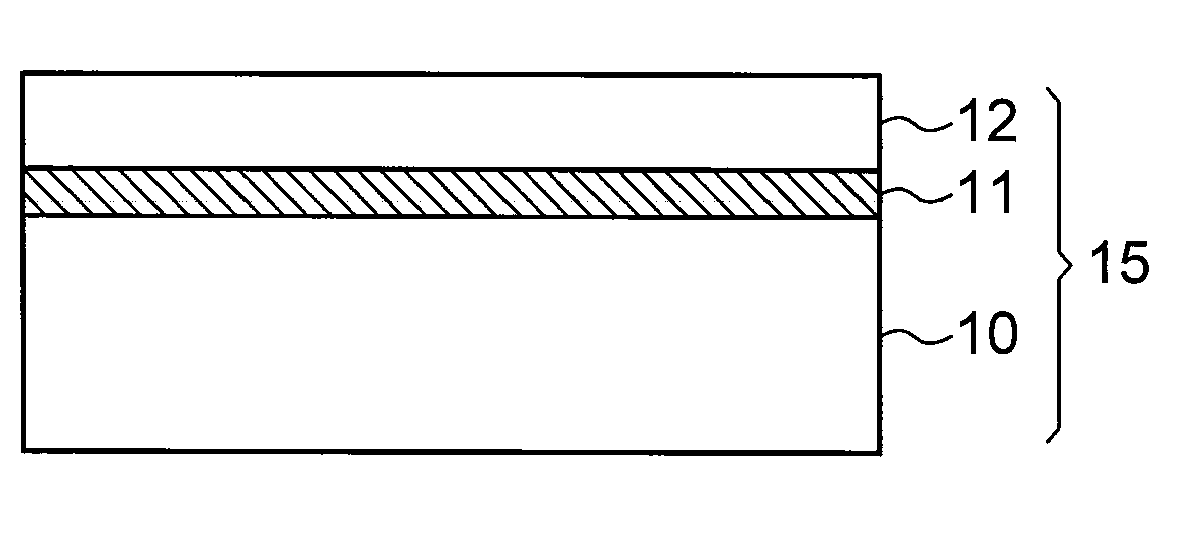
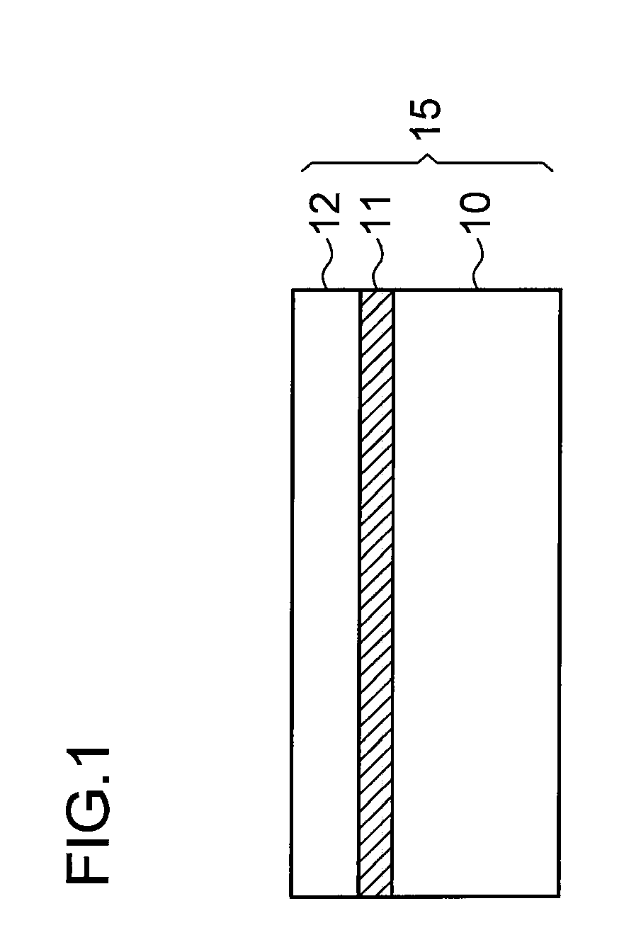
[0041]FIG. 1 is a cross-sectional view showing a zinc-oxide-based semiconductor crystal layer (hereinafter, simply referred to as a ZnO-based semiconductor layer) grown on a substrate 10 according to the present invention. More specifically, a ZnO layer 11 and a ZnO-based semiconductor layer 12 are grown on a sapphire substrate using the MOCVD method. Description will be made below taking as an example the case of growing MgxZn(1-x)O (0≦x≦0.68) as the ZnO-based semiconductor layer 12.

[0042]Note that the ZnO-based semiconductor may be another ZnO-based compound crystal, not being limited to MgxZn(1-x)O. For example, it may be a ZnO-based compound crystal having a portion of Zn (zinc) replaced by calcium (Ca), or a ZnO-based compound crystal having some of O (oxygen) replaced by selenium (Se), sulfur (S), tellurium (Te), or the like.

[0043]The MOCVD apparatus (not shown) used in crystal growth has a reaction container (chamber), and inside the reaction chamber, there are provided a sus...

embodiment 2

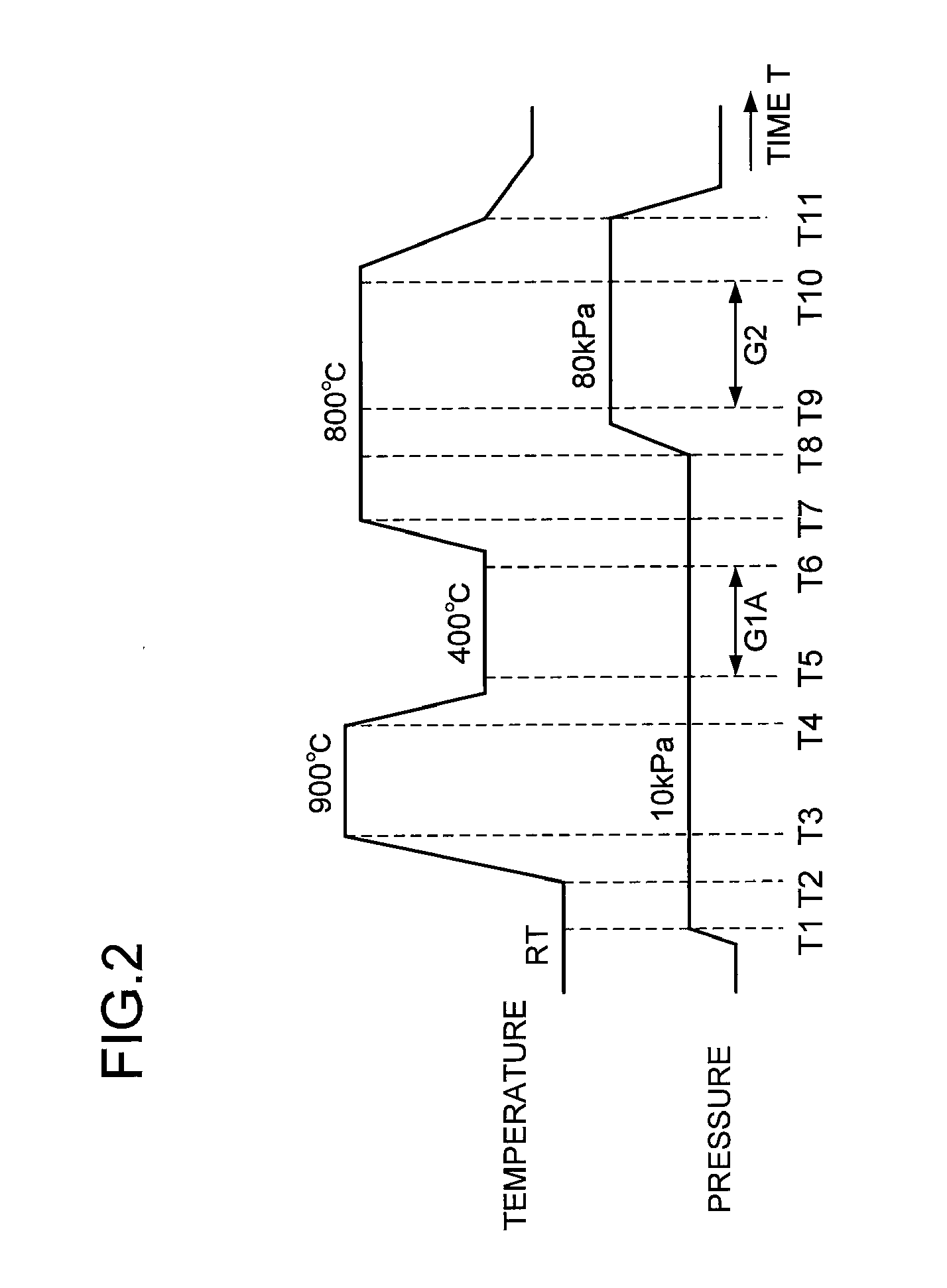
[0103]FIG. 9 is a cross-sectional view of a semiconductor light emitting device structure grown on the substrate 10 according to the present invention. More specifically, a light emitting operation layer (hereinafter also called an LED operation layer) 20 including an n-type ZnO-based semiconductor layer 21, a ZnO-based semiconductor active layer 22, and a p-type ZnO-based semiconductor layer 23 was formed on the with-grown-layer substrate 15 having the ZnO layer 11 and the ZnO-based semiconductor layer 12 formed thereon according to the above-described embodiment. Crystal growth conditions of the LED operation layer 20 were the same as those of the ZnO-based semiconductor layer 12 unless otherwise noted. That is, the crystal growth sequence was the same as that shown in FIG. 2, and using the same growth temperature, growth pressure, material gas, etc., as in the period (G2) of T=T9 to T10, the n-type ZnO-based semiconductor layer 21, ZnO-based semiconductor active layer 22, and p-t...

embodiment 3

[0129]FIG. 12 is a cross-sectional view of a zinc-oxide-based semiconductor crystal layer grown on the substrate 10 according to the present invention. More specifically, a first ZnO layer 11A, a second ZnO layer 11B, and a ZnO-based semiconductor layer 12 are formed on a sapphire substrate using the MOCVD method. Description will be made below taking as an example the case of growing MgxZn(1-x)O (0≦x≦0.68) as the ZnO-based semiconductor layer 12.

[0130]FIG. 13 shows a crystal growth sequence used in crystal growth by the MOCVD method. First, the A-plane sapphire substrate 10 was set on the susceptor in the MOCVD apparatus, and the reaction chamber pressure was adjusted to 10 kPa (kilopascals) (time T=T1).

[0131]Next, H2O (water vapor) as an oxygen source started to be supplied from the shower head to the substrate 10 at a flow rate of 640 μmol / min (T=T2). Further, the substrate 10 was raised in temperature by the heater from room temperature (RT) to 900° C. to perform the degassing o...


PUM


Abstract

A method includes the steps of, using water vapor and a metalorganic compound not containing oxygen, (a) performing crystal growth at a low growth temperature and at a low growth pressure in the range of 1 kPa to 30 kPa to form a low-temperature grown single-crystal layer; and (b) performing crystal growth at a high growth temperature and at a pressure higher than the low growth pressure to form a high-temperature grown single-crystal layer on the low-temperature grown single-crystal layer.

Description

BACKGROUND OF THE INVENTION[0001]1. Field of the Invention[0002]The present invention relates to a method of growing a zinc-oxide-based semiconductor and a method of manufacturing a semiconductor device, and particularly to a method of growing a zinc-oxide-based semiconductor layer by an MOCVD method and a method of manufacturing a semiconductor light emitting device using the method.[0003]2. Description of the Related Art[0004]Zinc oxide (ZnO) is a direct transition semiconductor having band gap energy of 3.37 eV at room temperature and expected to serve as a material for optical devices of a blue to ultraviolet range. In particular, the binding energy of excitons thereof being 60 meV with refractive index n=2.0, ZnO has physical properties extremely suitable for semiconductor light emitting devices. Further, not being limited to light emitting and light receiving devices, ZnO can be widely applied to surface acoustic wave (SAW) devices, piezoelectric devices, and the like. Moreove...

Claims


Application Information

Patent Timeline
IPC IPC(8): C30B25/00
CPCC30B29/16C30B25/02
Inventor HORIO, NAOCHIKAMAKISHIMA, MASAYUKI
Owner STANLEY ELECTRIC CO LTD
Learn More