

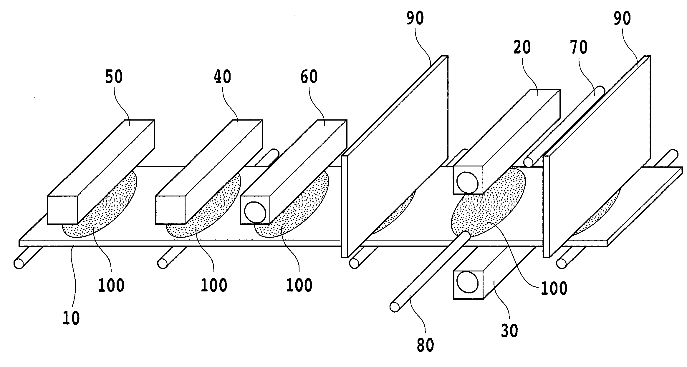
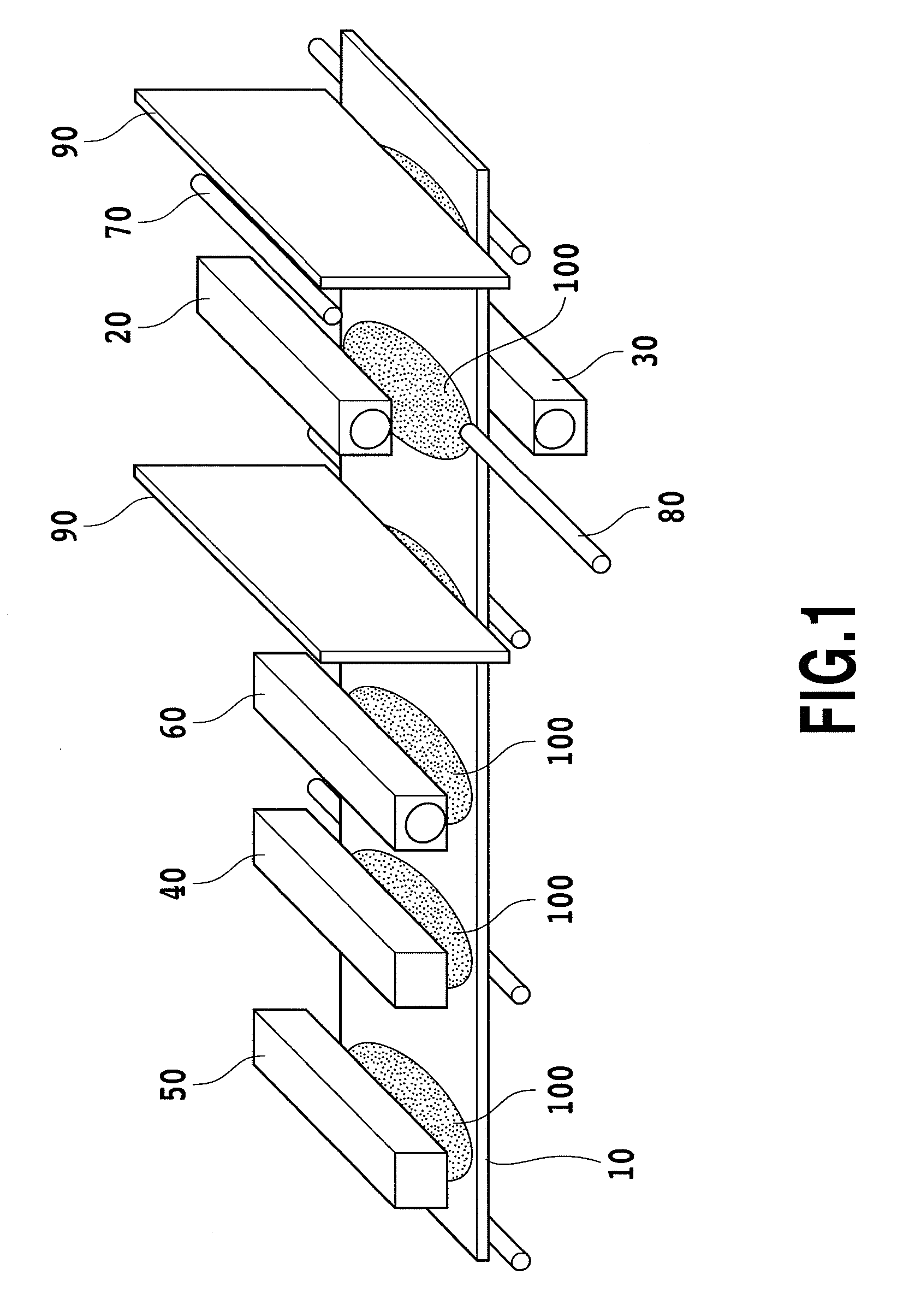
Apparatus for manufacturing silicon oxide thin film and method for forming the silicon oxide thin film
a technology of silicon oxide and silicon oxide, which is applied in the direction of coatings, basic electric elements, chemical vapor deposition coatings, etc., can solve the problems of deteriorating the electrical characteristics of the obtained film, the reaction product becomes imperfect, and the method cannot be used to fabricate electronic devices on such substrates through printing methods, etc., to achieve simple and low-cost, high plasticity, and high insulating performance
- Summary
- Abstract
- Description
- Claims
- Application Information
AI Technical Summary
Benefits of technology
Problems solved by technology
Method used
Image

Examples
example 1
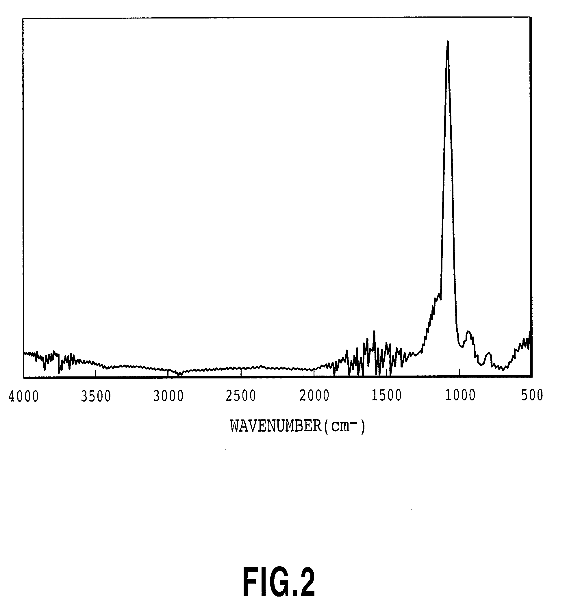
[0083]Poly(perhydrosilazane) was dissolved in a mixture solvent of dibutyl ether and cyclohexanone (mixture ratio: 2:5) to fabricate a solution at a concentration of approximately 6.7 wt %, which was used as a raw material solution for fabricating a thin coating film. A mirror-polished silicon wafer of 2 cm in diameter and 1 mm in thickness was used as a substrate on which a silicon oxide thin film was eventually fabricated. A surface cleaning by the method shown below was performed as a pre-treatment of the substrate. The substrate was flushed with ultrapure water for one minute to thereby remove substances attached to the surface. Thereafter, the water was removed by an air gun. Subsequently, the substrate was transferred into a plasma dry cleaner PDC 510 manufactured by Yamato Scientific Co., Ltd., and was subjected to an oxygen plasma treatment by a DP method for 3 minutes. The substrate was then immersed for 2 minutes in a hydrofluoric acid obtained through 100-fold dilution wi...
example 2
[0084]Poly (perhydrosilazane) was dissolved in a mixture solvent of dibutyl ether and cyclohexanone (mixture ratio: 2:5) to fabricate a solution at a concentration of approximately 6.7 wt o, which was used as a raw material solution for fabricating a thin coating film. A glass plate of 2 cm square with 1 mm thickness was used as a substrate on which a silicon oxide thin film was eventually fabricated. On a surface of the substrate, a chrome metal thin film had been fabricated by sputtering. A surface cleaning by the method shown below was performed as a pre-treatment on the substrate. The substrate was flushed with ultrapure water for one minute to thereby remove substances or the like attached to the surface. Thereafter, the water was removed by an air gun. Subsequently, the substrate was transferred into a plasma dry cleaner PDC 510 manufactured by Yamato Scientific Co., Ltd., and was subjected to an oxygen plasma treatment by a DP method for 3 minutes. The substrate was then imme...
example 3
[0085]Poly(perhydrosilazane) was dissolved in a mixture solvent of dibutyl ether and cyclohexanone (mixture ratio: 1:5) to fabricate a solution at a concentration of approximately 4.0 wt %, which was used as a raw material solution for fabricating a thin coating film. A glass plate of 2 cm square with 1 mm thickness was used as a substrate on which a silicon oxide thin film was eventually fabricated. On a surface of the substrate, a chrome metal thin film had been fabricated by sputtering. A surface cleaning by the method shown below was performed as a pre-treatment on the substrate. The substrate was passed into a Teflon (registered trademark) container containing a liquid crystal substrate cleaning liquid Semico Clean 23 manufactured by Furuuchi Chemical Corporation in an undiluted form, and then subjected to ultrasonic cleaning for 15 minutes. Thereafter, the substrate was passed into a Teflon (registered trademark) container containing ultrapure water, and then subjected to ultr...
PUM
| Property | Measurement | Unit |
|---|---|---|
| temperature | aaaaa | aaaaa |
| temperature | aaaaa | aaaaa |
| heat resistant temperatures | aaaaa | aaaaa |
Abstract
Description
Claims
Application Information