Optical element, exposure apparatus using this, and device manufacturing method

a technology of exposure apparatus and optical element, which is applied in the direction of photomechanical apparatus, instruments, printing, etc., can solve the problems of degrading the reaction reducing the imaging properties of the projection optical system, and reducing the life of the optical element, so as to maintain the reflective properties of the optical element over a long period, suppress the non-exposure light, and reduce the non-exposure light

Active Publication Date: 2010-07-29
NIKON CORP
View PDF8 Cites 17 Cited by
  • Summary
  • Abstract
  • Description
  • Claims
  • Application Information

AI Technical Summary

Benefits of technology

[0015]By using at least one of the aforementioned optical elements in the aforementioned exposure apparatus, it is possible to inhibit oxidation of the surface of the pertinent optical element inside the apparatus, thereby enabling maintenance of the reflective properties of the optical element over a long period. This means that the throughput of the exposure apparatus can be maintained over a long period, and that the exposure apparatus can be given a long life. By using the aforementioned optical elements, it is also possible to reduce non-exposure light, from the light source, that is unnecessary for exposure, and to suppress the non-exposure light that is received by the sensitive substrate or the like, thereby enabling achievement of a high-precision exposure apparatus.
[0016]Still another aspect of the present invention provides a device manufacturing method. In the method, it is possible to manufacture high-performance devices by using the aforementioned exposure apparatus in a manufacturing process.

Problems solved by technology

Due to this, the problem arises that reaction properties of the optical element are degraded, and that life is shortened.
Moreover, the light source that is employed by the exposure apparatus not only emits the extreme ultraviolet radiation required for exposure, but also non-exposure light that is unnecessary for exposure.
When non-exposure light is included in the source light, it engenders the problems of: (1) degradation of imaging properties of the projection optical system; (2) reduction in resolution of the pattern; and (3) generation of distortions in the alignment accuracy of the sensitive substrate.
This means that the throughput of the exposure apparatus can be maintained over a long period, and that the exposure apparatus can be given a long life.

Method used


Image

  • Optical element, exposure apparatus using this, and device manufacturing method
  • Optical element, exposure apparatus using this, and device manufacturing method
  • Optical element, exposure apparatus using this, and device manufacturing method

Examples


first embodiment

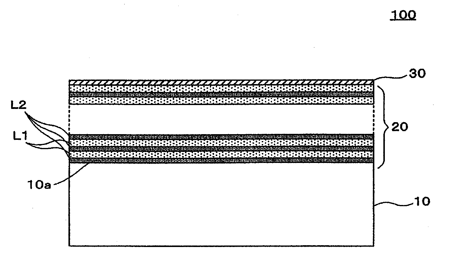
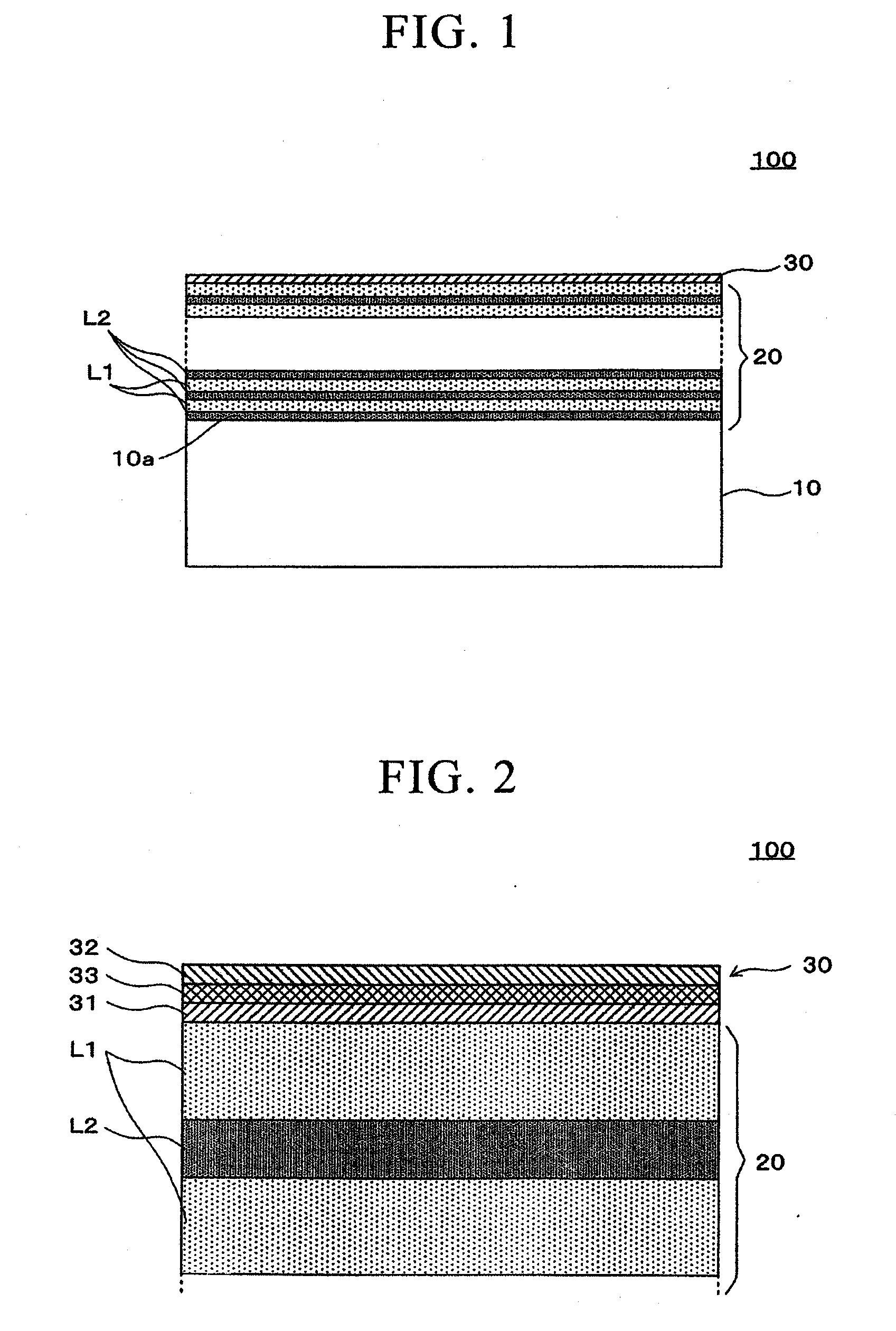
[0025]FIG. 1 is a cross-sectional view which shows the structure of the optical element pertaining to a first embodiment. The optical element 100 of the present embodiment is, for example, a flat mirror and has a substrate 10 that supports a multilayer film structure, a multilayer film 20 for reflection, and a protective layer 30 that constitutes the surface layer.

[0026]The underlying substrate 10 is formed, for example, by machining synthetic quartz glass or low-expansion glass, and its top face 10a is polished to a mirror surface of prescribed accuracy. The top face 10a may be made into a plane as illustrated in the drawing, or it may be made concave, convex, multifaceted or some other shape (not illustrated in the drawing) according to the application of the optical element 100.

[0027]The multilayer film 20 that is above is a thin film of from several layers to several hundred layers, and is formed by alternately laminating two types of materials having different refractive indice...

first example

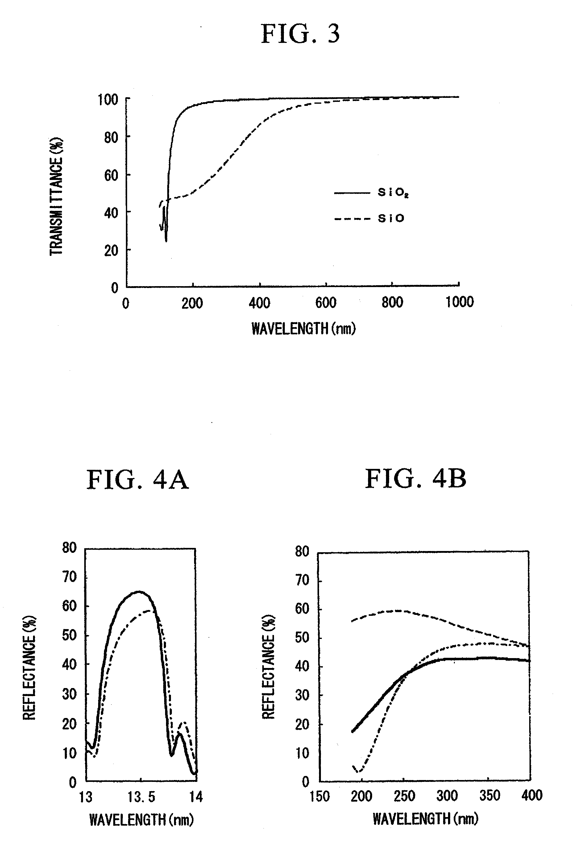
[0040]Below, a description is given of a specific working example of the optical element 100 pertaining to the first embodiment. “ULE”® (Ultra-Low Expansion), which is a low thermal expansion glass manufactured by Corning International Co., was used as the material of the substrate 10. One may also use other low thermal expansion glass instead of ULE, such as “Zerodur”® manufactured by Schott Co., and “CLEARCERAM-Z”® manufactured by Ohara Co. In order to prevent a reduction in reflectance due to surface roughness of the substrate 10, the surface of the substrate 10 is polished to a surface roughness of 0.3 nm RMS or less.

[0041]A multilayer film 20 of Mo / Si type was then formed by the sputtering method on the aforementioned substrate 10. In this case, the thin-film layer L1 was a Si layer with a small difference relative to a refractive index of 1, and its thickness was set to 4.6 nm. The thin-film layer L2 was a Mo layer with a large difference relative to a refractive index of 1, a...

second example

[0046]Below, a description is given of a specific second example of the optical element 100 pertaining to the first embodiment. It should be noted that the optical element 100 in the second example is a modified example of the first example. Substantial descriptions of elements that are identical to the elements of the first example are omitted.

[0047]In the second example, the protective layer 30 is provided on top of the Si layer (i.e., the topmost Si thin film layer L1) that is the topmost layer of the Mo / Si multilayer film 20 and that has a thickness of 3.2 nm. In the protective layer 30, the interfacial-side layer 31 consisting of SiO and having a thickness of 3.2 nm is formed, the intermediate layer 33 consisting of SiO1.5 and having a thickness of 3.2 nm is formed, and the surface-side layer 32 consisting of SiO2 and having a thickness of 3.2 nm is formed.

[0048]FIGS. 4A and 4B show reflection characteristics of the optical element 100 in the second example. In FIG. 4A, the sol...


PUM

PropertyMeasurementUnit
wavelengthsaaaaaaaaaa
sizeaaaaaaaaaa
refractive indexaaaaaaaaaa

Abstract

On a multilayer film mirror, a protective layer is formed having a varied composition in the depth direction. The protective layer includes an interface side layer formed on a thin film layer, i.e., the outermost layer of a multilayer film, a surface side layer provided on the interface side layer as the outermost surface of an optical element, and an intermediate layer. The interface side layer has properties such as providing relative absorption of non-exposure light from a light source. The surface side layer suppresses oxidation of the surface of the multilayer film.

Description

CROSS-REFERENCE TO RELATED APPLICATION[0001]This is a Continuation Application of International Application No. PCT / JP2008 / 051119, filed Jan. 25, 2008, which claims priority to Japanese Patent Application No. 2007-014920, filed Jan. 25, 2007. The contents of the aforementioned applications are incorporated herein by reference.BACKGROUND[0002]1. Field of the Invention[0003]The present invention relates to an optical element used for extreme ultraviolet radiation, an exposure apparatus using this, and a device manufacturing method.[0004]2. Description of Related Art[0005]In conjunction with the miniaturization of semiconductor integrated circuits in recent years, exposure technology has been developed which, instead of conventional ultraviolet radiation, uses extreme ultraviolet radiation composed of wavelengths (11-14 nm) that are shorter than this conventional radiation in order to enhance optical system resolution that is attained according to the diffraction limits of light. By th...

Claims


Application Information

Patent Timeline
Patent Type & Authority Applications(United States)
IPC IPC(8): G03F7/20G03B27/54G02B5/22
CPCB82Y10/00G02B5/0816G02B5/0891G02B5/26G02B17/0657G21K1/062G03F7/70316G03F7/70575G03F7/70916G03F7/70958G03F7/70308
Inventor MURAKAMI, KATSUHIKOKOMIYA, TAKAHARU
Owner NIKON CORP
Why Eureka
Try Eureka