Group iii nitride semiconductor light-emitting device, method for manufacturing the same, and lamp

Inactive Publication Date: 2010-09-02
SHOWA DENKO KK
View PDF6 Cites 84 Cited by
  • Summary
  • Abstract
  • Description
  • Claims
  • Application Information

AI Technical Summary

Benefits of technology

[0020]According to the Group III nitride semiconductor light-emitting device of the present invention, the buffer layer formed by means of a reactive sputtering method contains oxygen and the oxygen concentration in the buffer layer is 1 atomic percent

Problems solved by technology

Between such different types of substrates and Group III nitride semiconductor crystals epitaxially grown thereon, there is a considerable lattice misfit.
In general, there is a problem in that in those cases where there is a considerable lattice misfit as described above, it is difficult to epitaxially grow crystals directly on the substrate, and even if crystals are grown thereon, crystals with superior crystallinity cannot be obtained.
However, in the method disclosed in Patent Documents 1 and 2, a lattice misfit is present between the su

Method used


Image

  • Group iii nitride semiconductor light-emitting device, method for manufacturing the same, and lamp
  • Group iii nitride semiconductor light-emitting device, method for manufacturing the same, and lamp
  • Group iii nitride semiconductor light-emitting device, method for manufacturing the same, and lamp

Examples


example 1

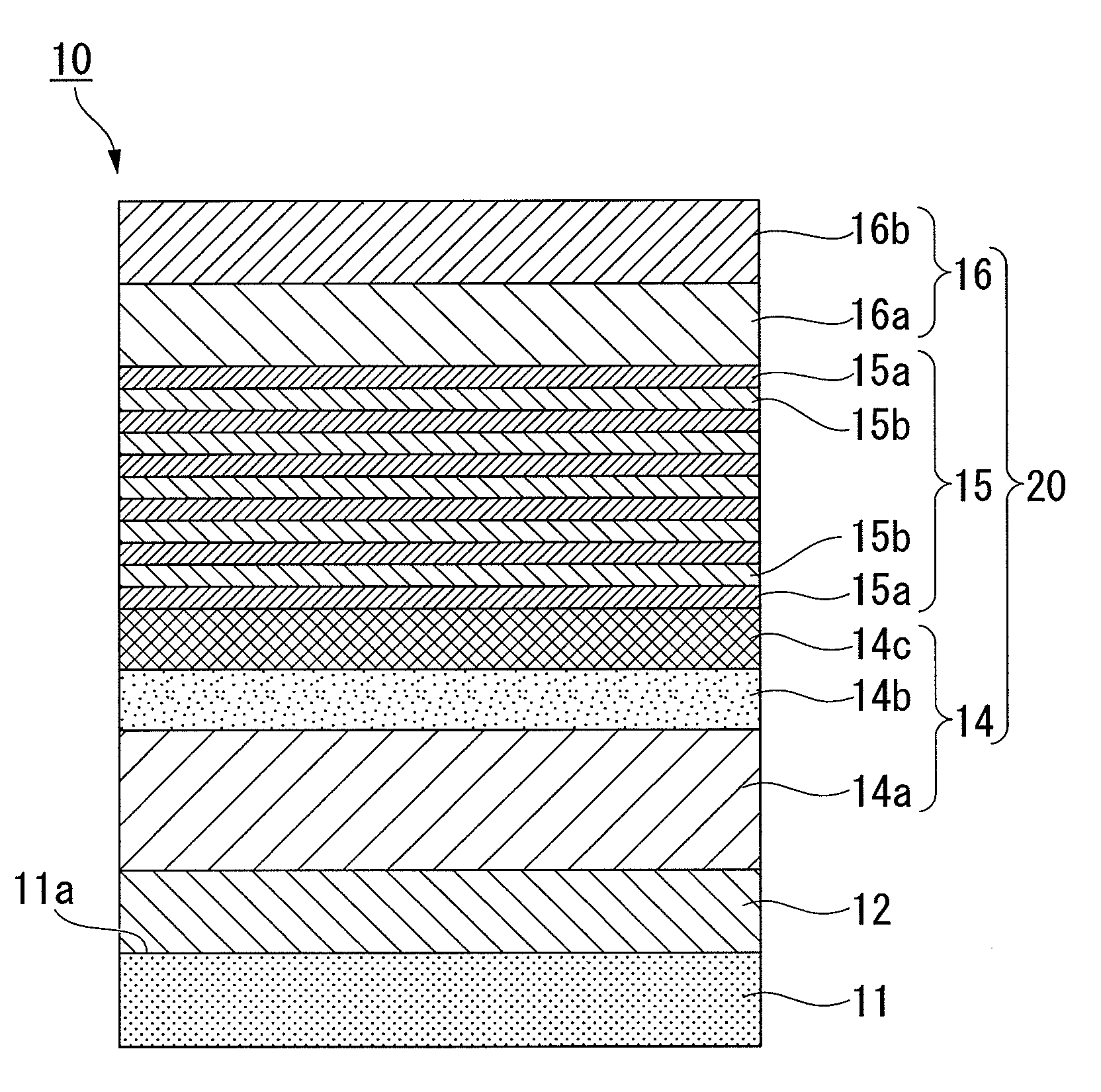
[0179]FIG. 1 shows a cross-sectional schematic view of the laminated semiconductor of the Group III nitride compound semiconductor light-emitting device manufactured in the present experimental example.

[0180]In the present example, on the c-plane of the substrate 11 composed of sapphire, there was formed, a single crystal layer composed of AlN that serves as the buffer layer 12, and on this, there was formed, by means of reactive sputtering, a layer composed of GaN (Group III nitride semiconductor) that serves as the base layer 14a.

“Formation of Buffer Layer”

[0181]First, a substrate formed of a 2-inch diameter (0001) c-plane sapphire that had been polished to a mirror surface was cleaned using a hydrofluoric acid and organic solvent, and then was placed inside a chamber. At this time, as the sputtering apparatus, as with the sputtering apparatus 40 illustrated in the example in FIG. 5, there was used an apparatus that has a high frequency type power supply and that has a mechanism ...

example 2

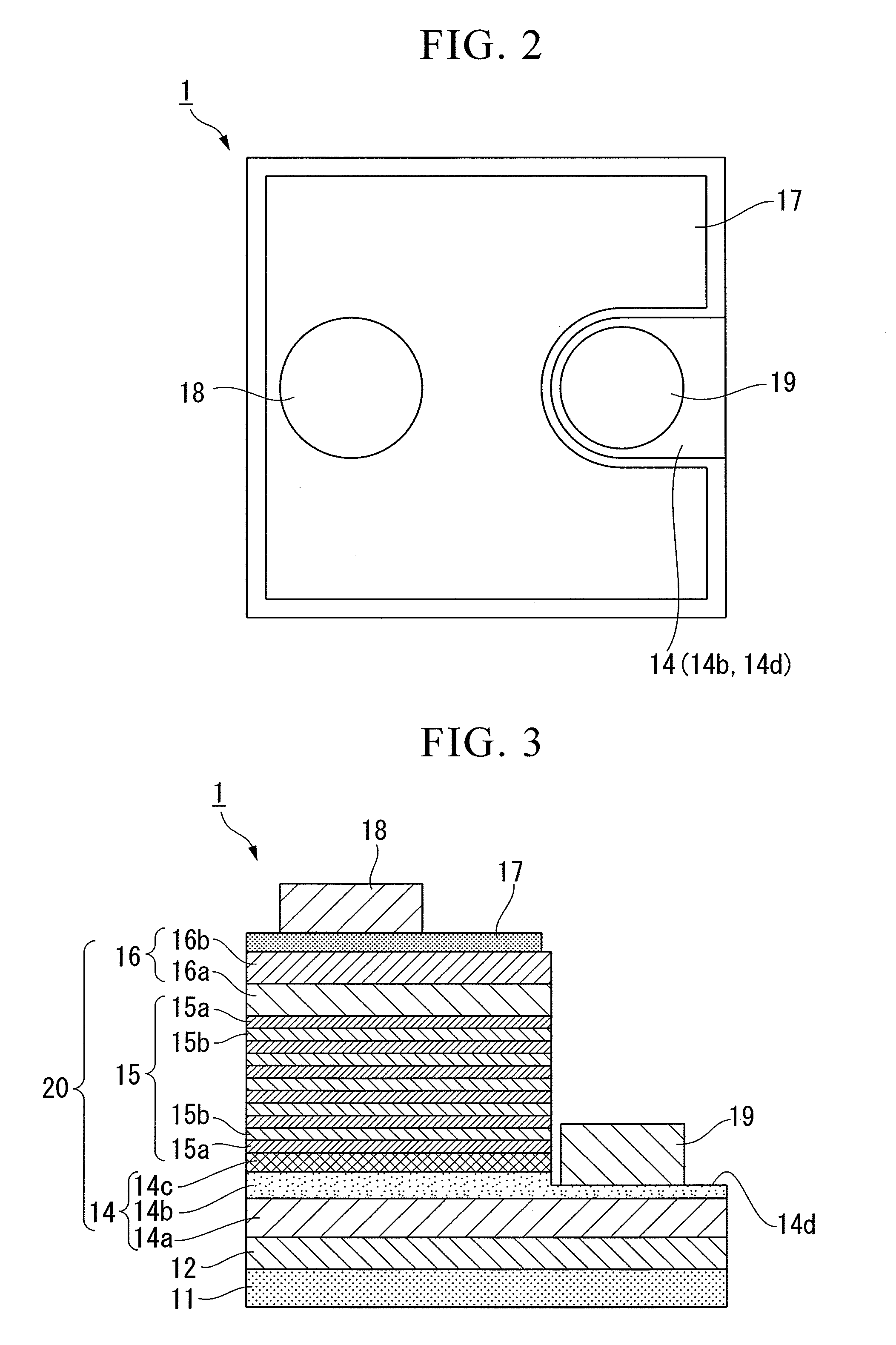
[0210]Using the same procedure as Example 1 above with the exception of using conditions where the crystal structure of a buffer layer to be formed on the substrate becomes a polycrystalline structure formed of a columnar crystal aggregate, the buffer layer was laminated on the substrate, an undoped GaN layer (a base layer) was laminated thereon, and respective layers composed of Group III nitride semiconductors were further formed, thereby producing a light-emitting device shown in FIG. 2 and FIG. 3.

[0211]When the X-ray rocking curve (XRC) of the buffer layer formed on the substrate was measured using the same method as Example 1, the XRC full width at half maximum was 12 arcsec. Moreover, the composition of the buffer layer was measured using an X-ray photoelectron spectroscopy apparatus (XPS), and as with Example 1, the measurement result confirmed that the oxygen concentration was 1 atomic percent or lower.

[0212]Using the same method as Example 1, a GaN layer was formed on the b...

experimental example

[0222]Hereunder, there is described, with reference to the respective graphs in FIG. 7A and FIG. 7B, an experimental example for substantiating the present invention. FIG. 7A is a graph showing a relationship between the number of dummy discharges and oxygen concentration in the buffer layer, and FIG. 7B is a graph showing a relationship between ultimate vacuum within the chamber and oxygen concentration within the buffer layer.

[0223]In the present experimental example, after conducting a pretreatment on the substrate, dummy discharging was performed the number of times shown in FIG. 7A when removing impurities by suctioning inside the chamber using a vacuum pump, and the ultimate vacuum was set to conditions shown in FIG. 7B (No. 1=2.0×10⁻⁵ Pa, No. 2=3.1×10⁻⁵ Pa, No. 3=5.1×10⁻⁵ Pa, No. 4=1.5×10⁻⁴ Pa). With the exception of this, the same method as Example 1 was used to manufacture respective samples No. 1 to 4 comprising a buffer layer formed on the substrate.

[0224]When the X-ray r...


PUM


Abstract

A buffer layer 12 composed of at least a Group III nitride compound is laminated on a substrate 11 composed of sapphire, and an n-type semiconductor layer 14, a light-emitting layer 15, and a p-type semiconductor layer 16 are laminated in a sequential manner on the buffer layer 12. The buffer layer 12 is formed by means of a reactive sputtering method, the buffer layer 12 contains oxygen, and the oxygen concentration in the buffer layer 12 is 1 atomic percent or lower. There are provided a Group III nitride compound semiconductor light-emitting device that comprises the buffer layer formed on the substrate by means of the reactive sputtering method, enables formation of a Group III nitride semiconductor having favorable crystallinity thereon, and has a superior light emission property, and a manufacturing method thereof, and a lamp.

Description

TECHNICAL FIELD[0001]The present invention relates to a Group III nitride semiconductor light-emitting device that is suitable for use in a light-emitting diode (LED), a laser diode (LD), an electronic device, or the like and that is prepared by laminating Group III nitride semiconductors expressed in a general formula AlaGabIncN (0≦a≦1, 0≦b≦1, 0≦c≦1, a+b+c=1), and to a method for manufacturing the device, and to a lamp.The present invention claims priority on Japanese Patent Application No. 2007-251478, the contents of which are incorporated herein by reference.BACKGROUND ART[0002]A Group III nitride semiconductor possess a band gap of a direction transition type of energy corresponding to the visible light through the ultraviolet light region and has an excellent level of light emission efficiency. Consequently, it has been commercialized as semiconductor light-emitting devices such as light-emitting diodes (LED), laser diodes (LD) and to be used in a variety of purposes. Also in ...

Claims


Application Information

Patent Timeline
IPC IPC(8): H01L33/30H01L33/00H01L33/06H01L33/12H01L33/20H01L33/32H01L33/40H01L33/56H01L33/62
CPCH01L33/025H01L33/06H01L33/12H01L33/32H01L2224/45144H01L2224/48257H01L2224/73265H01L2224/32245H01L2224/48091H01L2224/48247H01L2924/1305H01L2924/00014H01L2924/00H01L2924/181H01L2224/49107H01L2924/00012
Inventor YOKOYAMA, YASUNORIMIKI, HISAYUKI
Owner SHOWA DENKO KK
Why Eureka
Try Eureka