

Semiconductor device, single-crystal semiconductor thin film-including substrate, and production methods thereof
- Summary
- Abstract
- Description
- Claims
- Application Information
AI Technical Summary
Benefits of technology
Problems solved by technology
Method used
Image

Examples
embodiment 1
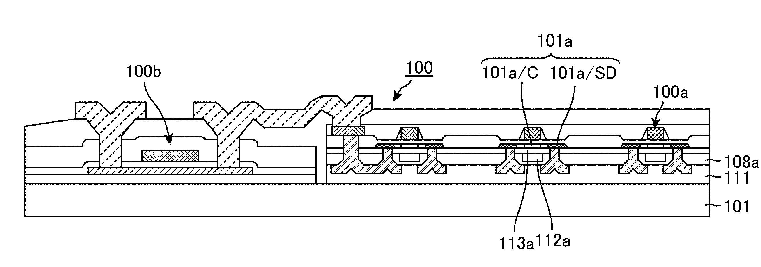
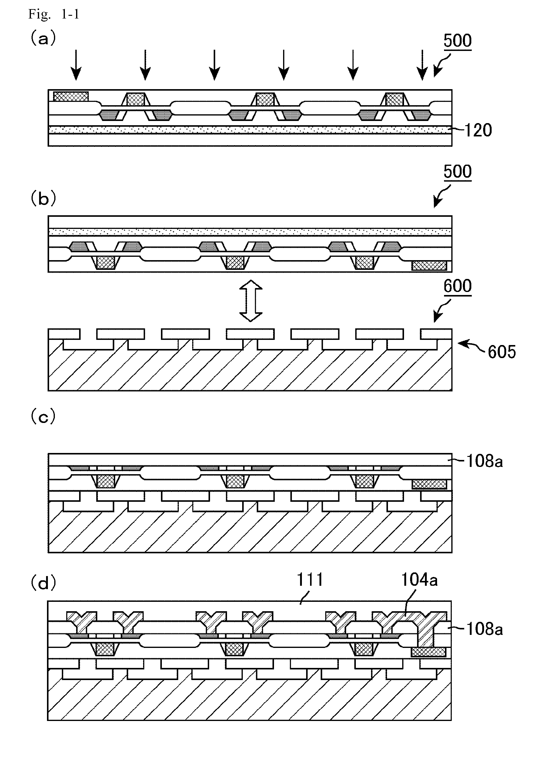
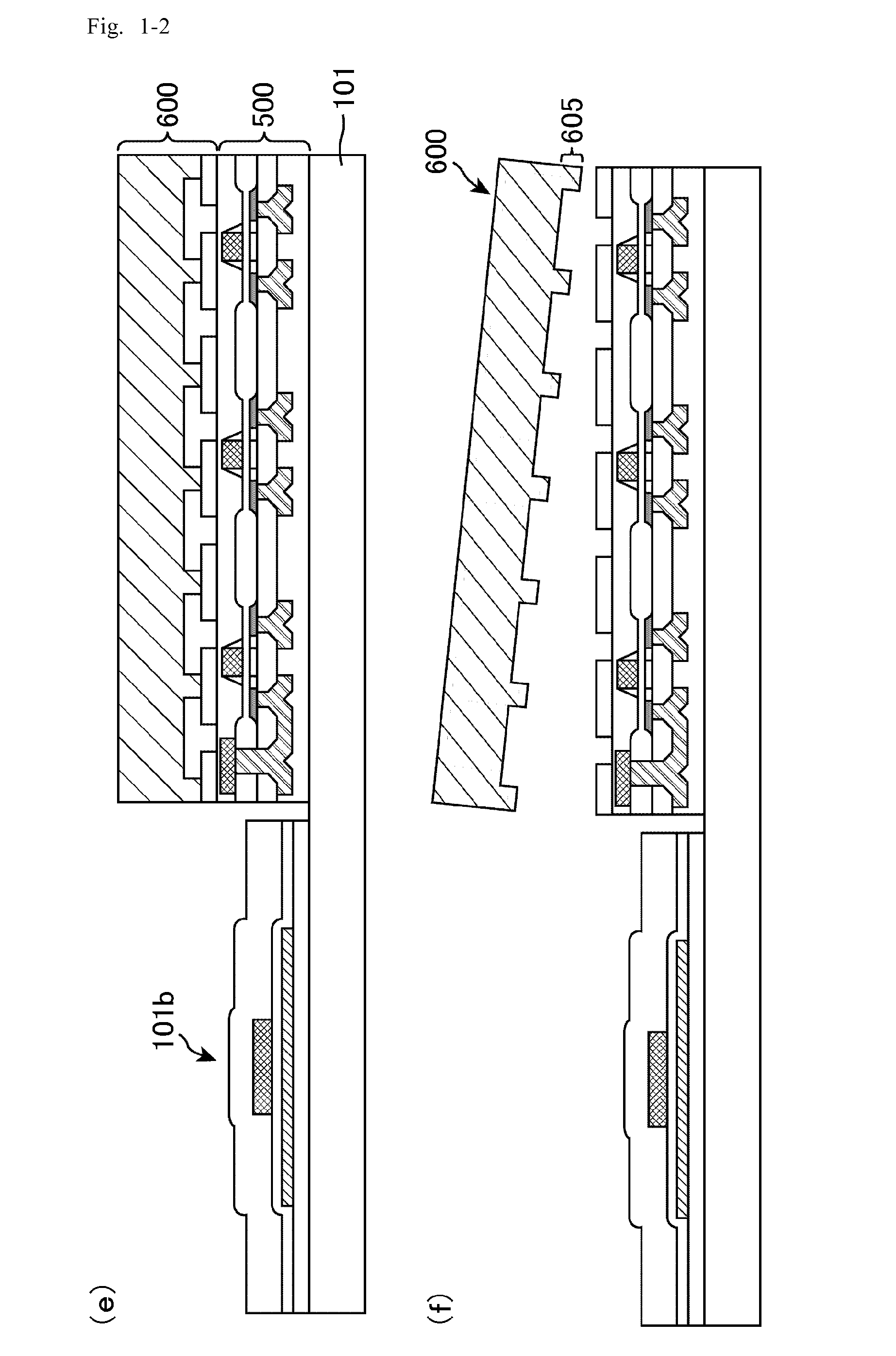
[0151]A single-crystal Si semiconductor device of Embodiment 1 and a production method thereof are mentioned below with reference to FIGS. 1-1 to 1-3 and FIGS. 2-1 to 2-3. FIGS. 1-1(a) to 1-1(d), FIGS. 1-2(e) and 1-2(f), and FIGS. 1-3(g) and 1-3(h) are cross-sectional views each schematically showing a production step of the semiconductor device of Embodiment 1. FIGS. 2-1 and 2-2 are schematic views each showing an intermediate substrate of Embodiment 1 in the production step. FIG. 2-1(a) is a plan view thereof. FIG. 2-1(b) is a cross-sectional view taken along line X1-X2 of FIG. 2-1(a). FIG. 2-2(a) is a plan view thereof. FIG. 2-2(b) is a cross-sectional view taken along line Y1-Y2 of FIG. 2-2(a). FIG. 2-3 is a schematic view showing a modified example of the intermediate substrate of Embodiment 1. FIG. 2-3(a) is a plan view thereof. FIG. 2-3(b) is a cross-sectional view taken along line Z1-Z2 of FIG. 2-2(a). In the plan views of FIGS. 2-1 to 2-3, the intermediate substrate has a r...
embodiment 2
[0208]A thin film semiconductor device including single-crystal strained Si of Embodiment 2 and a production method thereof are mentioned with reference to FIGS. 4-1 to 4-5. FIGS. 4-1(a) to 4-1(c), FIGS. 4-2(d) to 4-2(f), FIGS. 4-3(g) to 4-3(i), FIGS. 4-4(j) to 4-4(m), and FIGS. 4-5(n) to 4-5(p) are cross-sectional views each schematically showing a production step of the semiconductor device of Embodiment 2.
[0209]With reference to FIG. 4-1(a), a strained Si structure is mentioned first. A mixed crystal of GexSi1-x graded material is epitaxially grown (epi-growth) on a Si wafer (single-crystal Si substrate) 500 to form a graded layer (SiGe layer) 231 with 1 μm in thickness, and thereon, a GexSi1-x (SiGe mixed crystal) is grown to have a thickness of about 1 μm as a buffer layer (buffer GeSi layer) 232. As a result, dislocation-free GexSi1-x is grown. Further, thereon a Si layer with a thickness of about 10 nm to 20 nm is epitaxially grown, thereby growing a stained Si layer 201a, wh...
embodiment 3
[0235]A thin film semiconductor device including single-crystal Si of Embodiment 3 and a production method thereof are mentioned with reference to FIGS. 5-1 to 5-5 below. FIGS. 5-1(a) and 5-1(b), FIGS. 5-2(c) to 5-2(e) FIGS. 5-3(f) to 5-3(h), FIGS. 5-4(i) to 5-4(l), and FIGS. 5-5(m) to 5-5(o) are cross-sectional views schematically showing the semiconductor device of Embodiment 3.
[0236]A thermal oxide film 311 with a thickness of 50 nm is formed on a Si wafer (single-crystal Si substrate) 500 surface, first.
[0237]As shown in FIG. 5-1(a), cleavage substances, or hydrogen ions are implanted into the single-crystal Si layer so that the peak of the hydrogen ions is positioned at a predetermined depth, whereby a hydrogen ion-implanted portion (cleavage layer) 320 is formed (cleavage layer-forming step). The cleavage substances may be rare gas ion, in addition to H ion and H2 ion. Further, H2 ion may be used in combination with rare gas ion.
[0238]Referring to FIGS. 5-1(b) and 5-2(c), this...
PUM
 Abstract
Description
Claims
Application Information