Method of Depositing Silicon Oxide Film by Plasma Enhanced Atomic Layer Deposition at Low Temperature

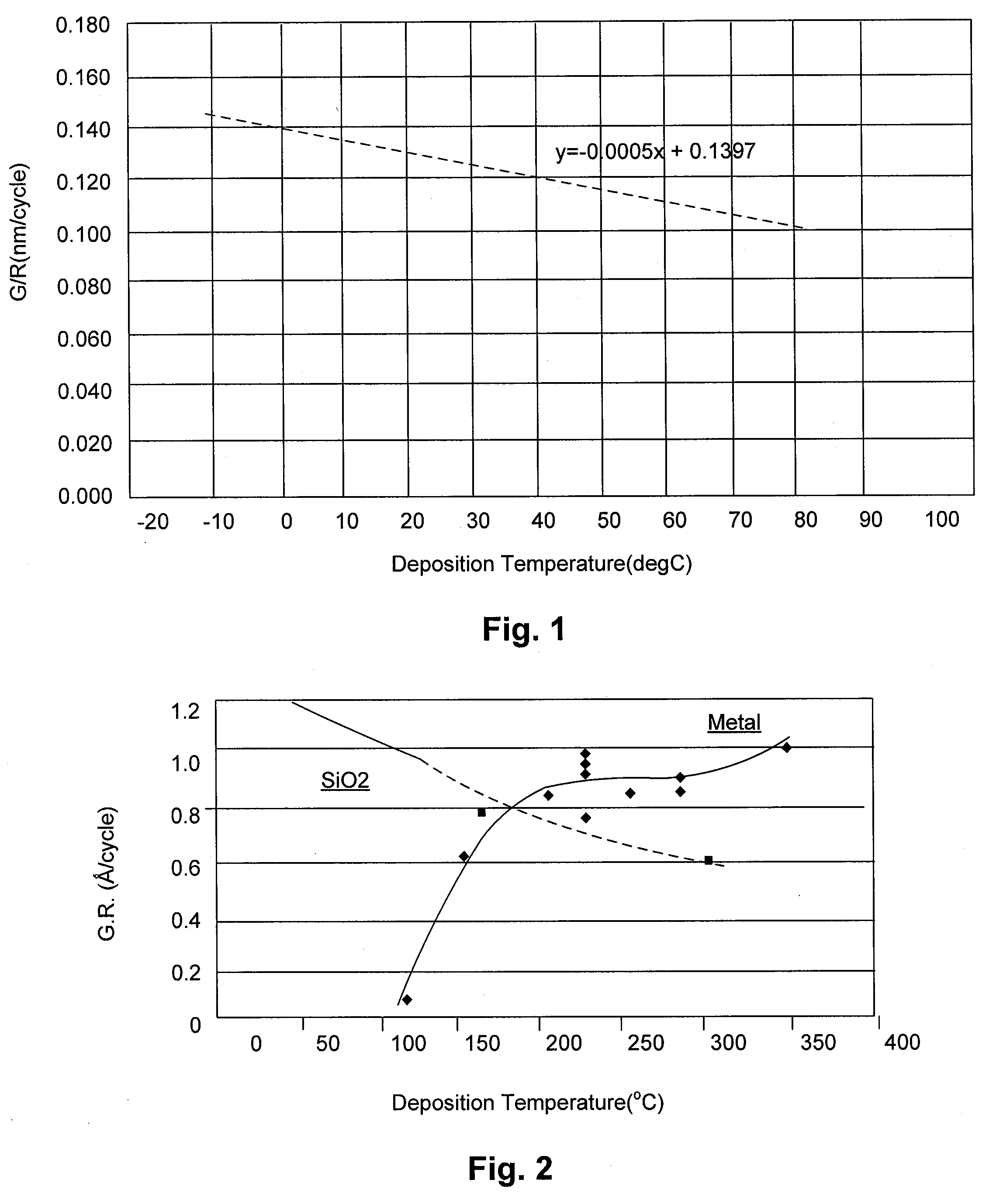
a technology of atomic layer deposition and plasma, which is applied in the field of depositing silicon oxide films by plasma enhanced atomic layer deposition, can solve the problems of inability to achieve temperature stability and repeatability in the process, and difficult temperature control using conventional susceptor heaters, so as to achieve effective inhibition, high film deposition speed, and further reduce the effect of film deposition temperatur

Active Publication Date: 2010-10-07
ASM JAPAN
View PDF7 Cites 376 Cited by
  • Summary
  • Abstract
  • Description
  • Claims
  • Application Information

AI Technical Summary

Benefits of technology

[0005]In an embodiment of the present invention, damage and deformation of the organic film on the substrate can be inhibited in the process of building a laminated structure on the substrate via PEALD, thereby enabling advanced, fine patterns to be created by means of lithography. In an embodiment of the present invention, a conformal silicon oxide film can be formed at high film deposition speed. In an embodiment that achieves at least one of the above, a silicon oxide film is deposited on a patterned organic film formed by PEALD, wherein the embodiment is characterized in that the film deposition speed is controlled as a linear function of the film deposition temperature in a region where the film deposition temperature is low. In an embodiment, damage and deformation of the organic film can be effectively inhibited in the SiO2 PEALD film deposition process by controlling the film deposition temperature at a constant level below 50° C. or so, or preferably at approx. 40° C. or below, or more preferably at approx. 30° C. or below. According to an experiment carried out by the inventor, in some cases the resist shape deformed due to damage, even at 50° C., and therefore it is desirable to lower the film deposition temperature further. At a constant temperature of approx. 30° C. or below, damage can be virtually prevented regardless of the type of resist. In this temperature region, it is possible to virtually control the film deposition speed as a complete linear function or roughly linear function of the film deposition temperature, in which case controlling the film thickness and film deposition time becomes markedly simple and the throughput can be improved. Surprisingly, the film deposition speed is a negative linear function of the film deposition temperature.
[0007]In the above, temperature control is difficult using conventional susceptor heaters if the PEALD method is used to deposit a SiO2 film at low temperatures of below 50° C. With any conventional susceptor heater, approx. 50° C. is the limit of temperature control and therefore the heater must be turned off and the process implemented at room temperature if a film must be deposited at lower temperatures. Since no heater or other similar mechanism is used, however, temperature stability and repeatability cannot be achieved in the process implemented in a normal temperature range of approx. 20 to 30° C. In an embodiment of the present invention, a structure with a chiller unit is used to circulate coolant inside the susceptor and thereby enable heating and cooling. This way, temperature control over a range of, say, −10 to 50° C. (or temperature control range of −10 to 80° C.) becomes possible and a film can be deposited at low temperature with good repeatability.

Problems solved by technology

Various types of resist are available, but all these resist materials are organic substances and therefore disappear at high temperature, which poses a problem.
In the above, temperature control is difficult using conventional susceptor heaters if the PEALD method is used to deposit a SiO2 film at low temperatures of below 50° C. With any conventional susceptor heater, approx.
Since no heater or other similar mechanism is used, however, temperature stability and repeatability cannot be achieved in the process implemented in a normal temperature range of approx.

Method used


Image

  • Method of Depositing Silicon Oxide Film by Plasma Enhanced Atomic Layer Deposition at Low Temperature
  • Method of Depositing Silicon Oxide Film by Plasma Enhanced Atomic Layer Deposition at Low Temperature
  • Method of Depositing Silicon Oxide Film by Plasma Enhanced Atomic Layer Deposition at Low Temperature

Examples


example

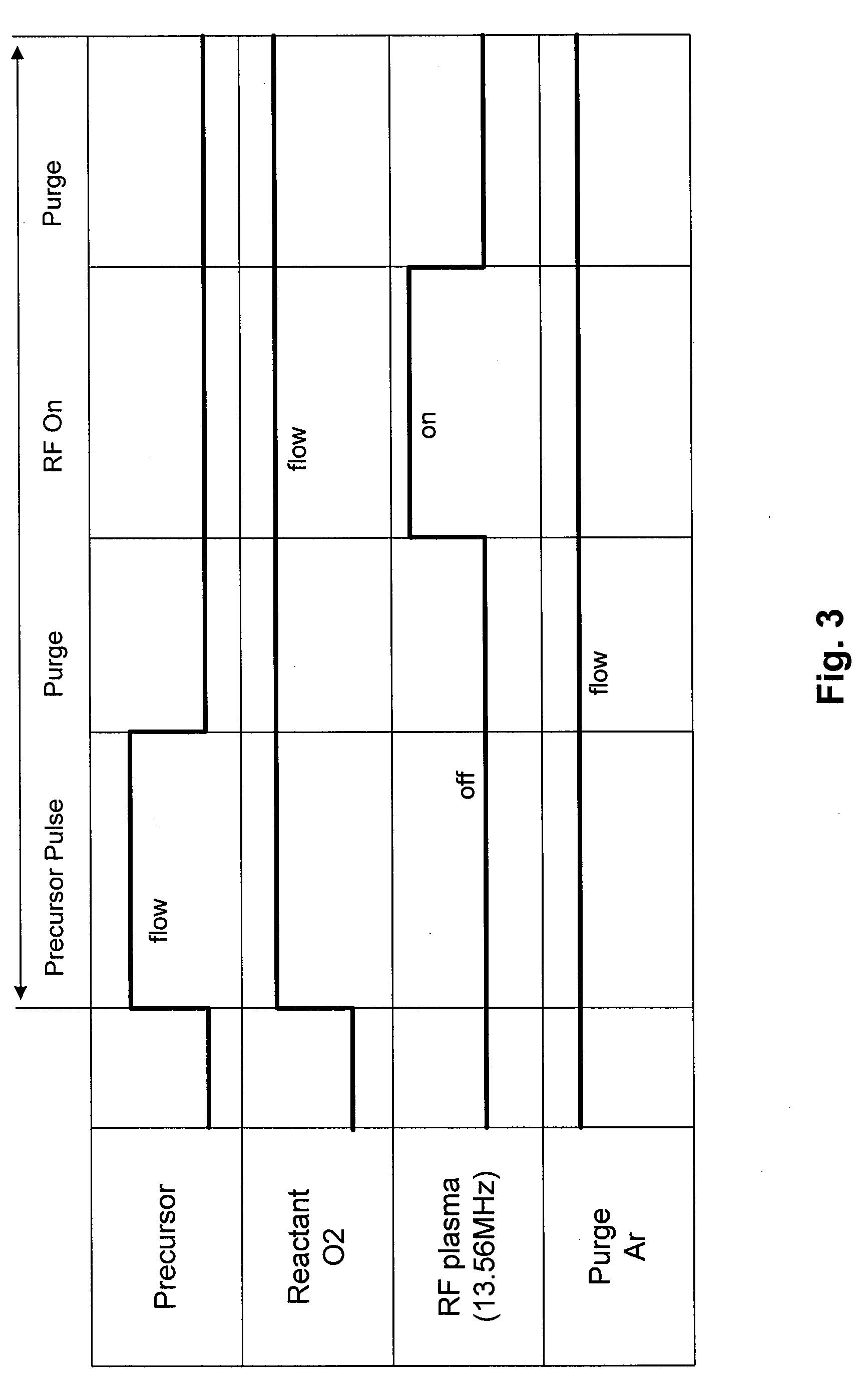
[0054]Three types of photoresist A, B and C (line width 40 nm, thickness 120 nm) were formed on substrates, as organic films, where the photoresist films for ArF laser had a structural composition based on an alkyl substitution product of acrylate or methacrylate ester polymer or copolymer, after which a SiO2 film was deposited by PEALD on top. The film deposition conditions were as follows:

[0055]Silicon-containing precursor: BDEAS

[0056]Flow rate of silicon-containing precursor: 500 sccm

[0057]Silicon-containing precursor pulse: 0.5 sec

[0058]Flow rate of oxygen: 600 sccm

[0059]Flow rate of Ar: 1.5 sccm

[0060]RF power (13.56 MHz): 50 W

[0061]RF power pulse: 0.3 sec

[0062]Interval between silicon-containing precursor pulse and RF power pulse (purge before application of RF power): 0.3 sec

[0063]Interval between RF power pulse and silicon-containing precursor pulse (purge after application of RF power): 0.3 sec

[0064]Film deposition pressure: 400 Pa

[0065]Duration of one cycle: 1.5 sec

[0066]As...


PUM

PropertyMeasurementUnit
temperatureaaaaaaaaaa

Abstract

A method of depositing a silicon oxide film on a resist pattern or etched lines formed on a substrate by plasma enhanced atomic layer deposition (PEALD) includes: providing a substrate on which a resist pattern or etched lines are formed in a PEALD reactor; controlling a temperature of a susceptor on which the substrate is placed at less than 50° C. as a deposition temperature; introducing a silicon-containing precursor and an oxygen-supplying reactant to the PEALD reactor and applying RF power therein in a cycle, while the deposition temperature is controlled substantially or nearly at a constant temperature of less than 50° C., thereby depositing a silicon oxide atomic layer on the resist pattern or etched lines; and repeating the cycle multiple times substantially or nearly at the constant temperature to deposit a silicon oxide atomic film on the resist pattern or etched lines.

Description

BACKGROUND[0001]1. Field of the Invention[0002]The present invention relates generally to a method of depositing a silicon oxide film by plasma enhanced atomic layer deposition (PEALD), and particularly, to a method of inhibiting deformation of an organic film such as a resist due to damage caused during film formation by PEALD.[0003]2. Description of the Related Art[0004]Traditionally atomic layer deposition (ALD) of SiO2 film involves deposition of film at approx. 300° C. In recent years, however, the demand for depositing a conformal SiO2 film on resist is increasing in order to support patterns finer than the lithography resolution required by increasingly integrated devices. Various types of resist are available, but all these resist materials are organic substances and therefore disappear at high temperature, which poses a problem.SUMMARY[0005]In an embodiment of the present invention, damage and deformation of the organic film on the substrate can be inhibited in the process ...

Claims


Application Information

Patent Timeline
Patent Type & Authority Applications(United States)
IPC IPC(8): B05D7/24
CPCC23C16/402C23C16/45542G03F7/40H01L21/32139H01L21/02274H01L21/0228H01L21/0337H01L21/02164
Inventor OKA, TAKAHIROSHIMIZU, AKIRA
Owner ASM JAPAN
Why Eureka
Try Eureka