Monolayer and/or Few-Layer Graphene On Metal or Metal-Coated Substrates

a graphene and metal coating technology, applied in the direction of metal/metal-oxide/metal-hydroxide catalysts, conductive materials, particle separator tubes, etc., can solve the problems of inability to efficiently and reproducibly form large (>100 m) single crystal domains in quantities sufficient for large-scale fabrication, and the formation of graphene domains with uniform thickness and length scales sufficient for practical applications remains a challeng

Inactive Publication Date: 2010-10-07
BROOKHAVEN SCI ASSOCS
View PDF4 Cites 109 Cited by
  • Summary
  • Abstract
  • Description
  • Claims
  • Application Information

AI Technical Summary

Benefits of technology

[0014]In yet another embodiment, second and subsequent layers of graphene nucleate and grow on top of or beneath the preceding layer. The outer layers of such a stack are more loosely bound to the transition metal substrate, thereby facilitating their removal for incorporation in practical applications. These outer graphene layers also exhibit properties more characteristic of free-standing graphene. Transfer of graphene layers may be accomplished by any of a plurality of techniques which may include, for example, oxide overgrowth and removal of the transition metal substrate by etching, or by intercalating a material between a first graphene layer covalently bonded to the transition metal and the metal and then removing the graphene layer.

Problems solved by technology

However, each of these methods suffers from a number of drawbacks, including an inability to efficiently and reproducibly form large (>100 μm) single-crystal domains in quantities sufficient for large-scale fabrication.
Consequently, the formation of graphene domains with uniform thicknesses and length scales sufficient for practical applications remains a challenge.

Method used


Image

  • Monolayer and/or Few-Layer Graphene On Metal or Metal-Coated Substrates
  • Monolayer and/or Few-Layer Graphene On Metal or Metal-Coated Substrates
  • Monolayer and/or Few-Layer Graphene On Metal or Metal-Coated Substrates

Examples


exemplary embodiment 1

I. Exemplary Embodiment 1

Growth on Single Crystal Substrates

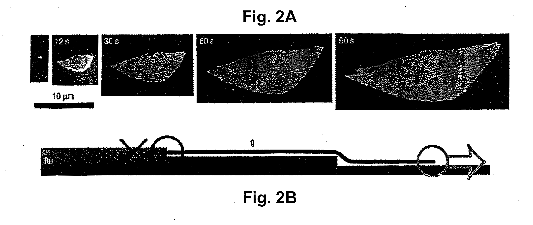
[0096]An exemplary method of forming graphene will now be described in detail. It is to be understood, however, that graphene growth is not limited to the method as described below, but may be accomplished by variations of the present method or by other, equivalent methods. A 99.999% pure Ru(0001) substrate with a miscut of 0.1° was initially cleaned ex situ by ultrasonication in acetone and then isopropyl alcohol followed by a 20 min rinse in deionized water. The substrate was then introduced into an UHV process chamber by means of a suitable load-lock and sample transfer system. A suitable choice of process chamber may be located within an Elmitec LEEM V field-emission LEEM with a sample stage capable of attaining temperatures ranging from 200 K to over 1500 K at pressures from UHV (≦Ton) to over 10−6 Torr. The LEEM may be equipped for in situ sample analysis using bright / dark field imaging, photoexcitation electron micro...

exemplary embodiment 2

II. Exemplary Embodiment 2

Growth on Planar Thin Films

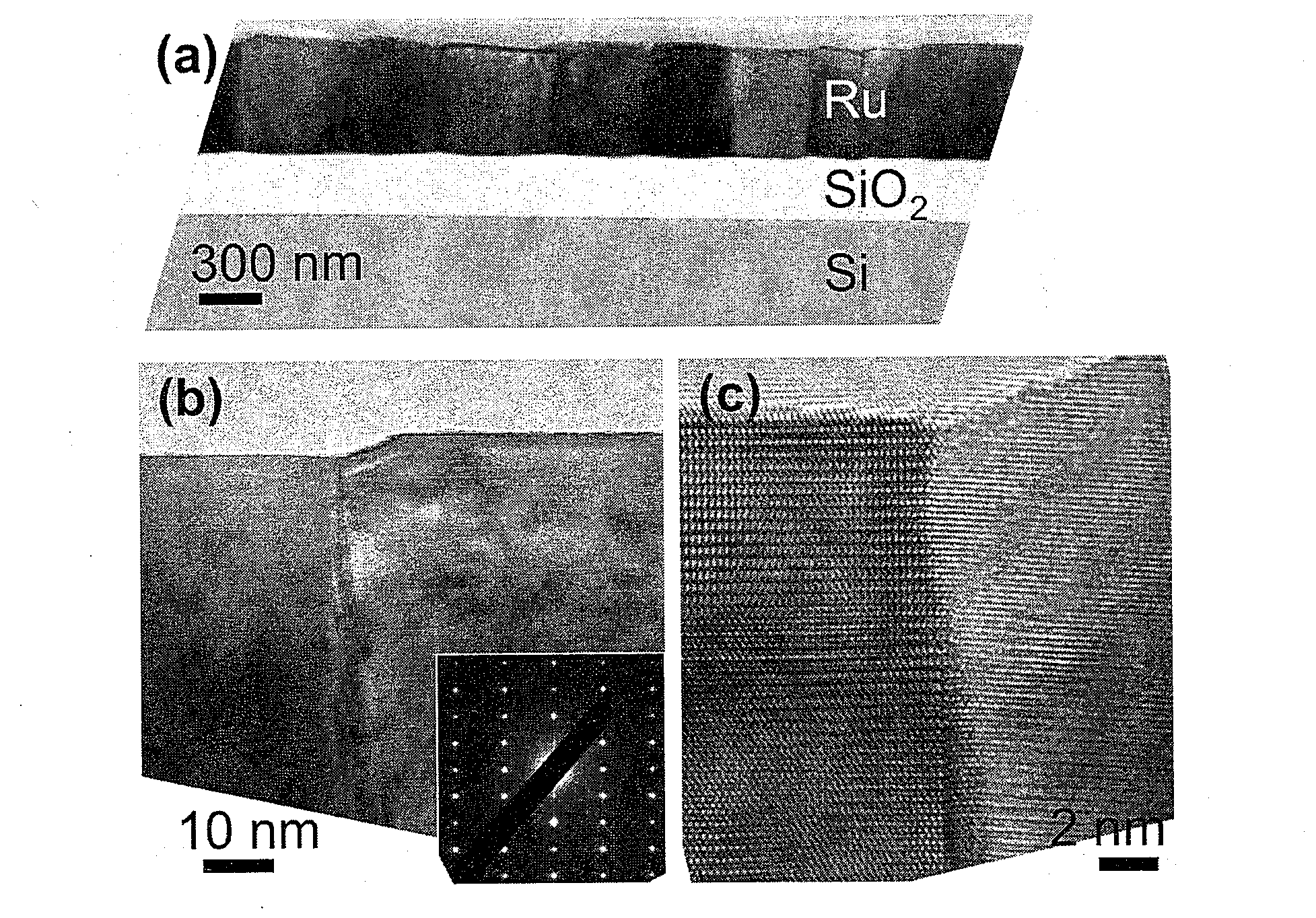
[0118]Polycrystalline Ru films with thicknesses ranging from 50 to 500 nm were grown on well degassed SiO2(300 nm) / Si substrates by rf magnetron sputtering of a Ru target (99.95% purity) in an UHV system with a base pressure of 2×10⁻¹⁰ torr. The substrate temperature during the Ru film deposition was 700° C. and the growth rate 0.06 nm / s. Following the growth, the Ru films were annealed at 950° C. in UHV for 20 min. Graphene epitaxy on Ru films was performed as on Ru(0001) single crystals, described in detail above. Briefly, the Ru thin films were enriched with interstitial C by exposure to ethylene (5×10⁻⁷ torr) at 950° C., followed by slow cooling in UHV to 550° C. The gradual lowering of the temperature reduces the C solubility in the Ru film and causes C segregation, driving graphene nucleation and growth at the surface. The morphology of the Ru films and the graphene layer were investigated in situ by STM in a microscope atta...

exemplary embodiment 3

III. Exemplary Embodiment 3

Growth on Non-Planar Thin Films

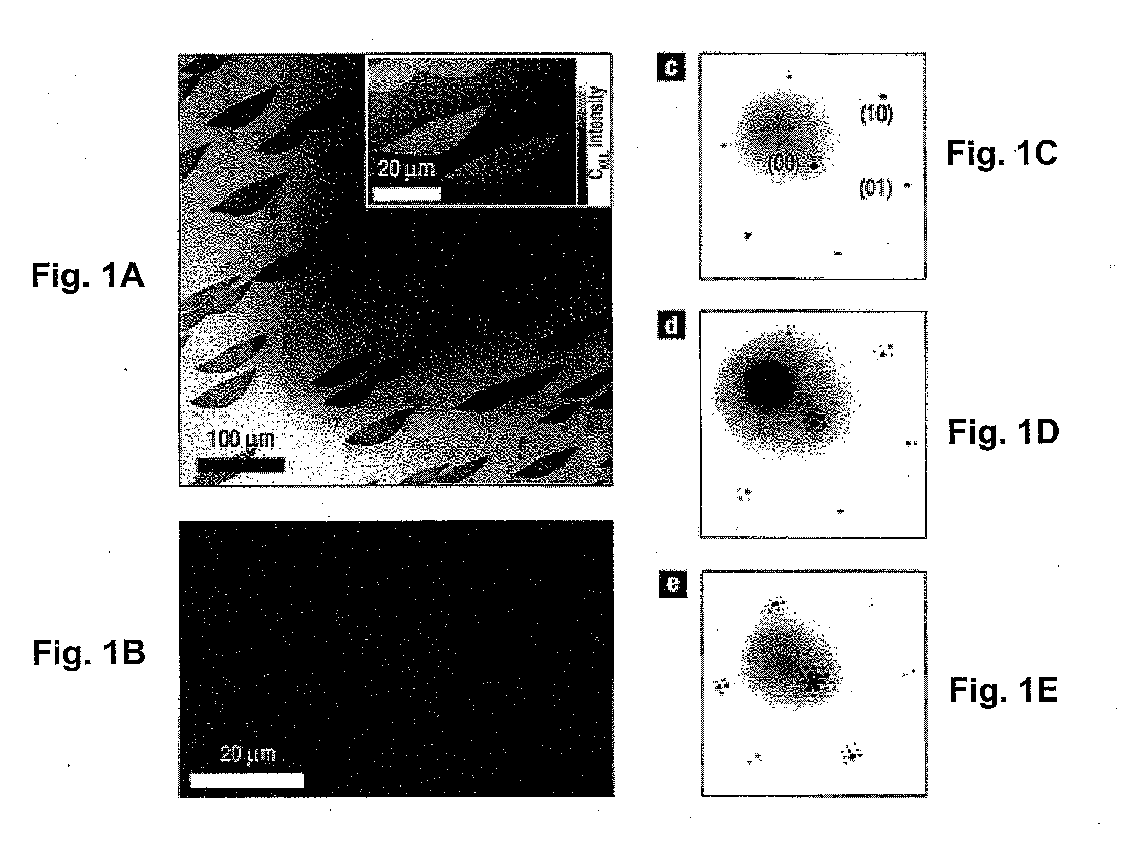
[0125]Arrays of three-dimensional geometric indents with different shapes—inverted tetrahedrons, square pyramids, and hemispheres—were designed and micromachined in fused silica substrates by focused ion beam (FIB). FIGS. 9A through 9C are micrographs of 3D geometrical indented patterns prepared by FIB milling. In FIGS. 9A and 9B the images were taken in a scanning electron microscope at a tilt of 52° with respect to the horizontal axis; the scale bars correspond to 5 μm. The left panel of FIG. 9A shows an inverted tetrahedron while the right panel shows an inverted square pyramid. Both were milled on a silicon substrate. Similar results, not shown, were obtained on fused silica substrates. FIG. 9B shows an inverted spherical cap milled in a fused silica substrate. The grain structure at the flat surface corresponds to the Au coating needed to reduce charging effects during milling. FIG. 9C is an optical micrograph of an arra...


PUM

PropertyMeasurementUnit
radiusaaaaaaaaaa
TMaaaaaaaaaa
TMaaaaaaaaaa

Abstract

Graphene is a single atomic layer of sp2-bonded C atoms densely packed into a two-dimensional honeycomb crystal lattice. A method of forming structurally perfect and defect-free graphene films comprising individual mono crystalline domains with in-plane lateral dimensions of up to 200 μm or more is presented. This is accomplished by controlling the temperature-dependent solubility of interstitial C of a transition metal substrate having a suitable surface structure. At elevated temperatures, C is incorporated into the bulk at higher concentrations. As the substrate is cooled, a lowering of the interstitial C solubility drives a significant amount of C atoms to the surface where graphene islands nucleate and gradually increase in size with continued cooling. Ru(0001) is selected as a model system and electron microscopy is used to observe graphene growth during cooling from elevated temperatures. With controlled cooling, large arrays of macroscopic single-crystalline graphene domains covering the entire transition metal surface are produced. As the graphene domains coalesce to a complete layer, a second graphene layer is formed, etc. By controlling the interstitial C concentration and the cooling rate, graphene layers with thickness up to 10 atomic layers or more are formed in a controlled, layer-by-layer fashion.

Description

[0001]This invention was made with Government support under contract number DE-AC02-98CH10886, awarded by the U.S. Department of Energy. The Government has certain rights in the invention.BACKGROUND[0002]I. Field of the Invention[0003]This invention relates generally to the formation of graphene. In particular, the present invention relates to the growth of large-area, structurally perfect monolayer and / or few-layer graphene domains on metal or metal-decorated substrates. In this context, “few-layer graphene” should be understood as a number of graphene layers stacked atop one another that continue to display the unique properties of graphene rather than those of graphite. This invention further relates to the utilization of the as-produced graphene layers in electronic devices, as sensors, as catalysts, or for mechanical purposes.[0004]II. Background of the Related Art[0005]Theoretical analyses have previously been used to demonstrate that two-dimensional (2D) crystal structures ar...

Claims


Application Information

Patent Timeline
Patent Type & Authority Applications(United States)
IPC IPC(8): B01J21/18C01B31/04H01B1/04H01B1/02B01J23/46B32B5/00G02B5/10H01J3/14
CPCB82Y30/00B82Y40/00C01B31/0461C01B2204/04H05H3/00G02B5/10H01J2201/30461H01J3/14G02B1/105C01B32/188G02B1/14
Inventor SUTTER, PETER WERNERSUTTER, ELI ANGUELOVA
Owner BROOKHAVEN SCI ASSOCS
Why Eureka
Try Eureka