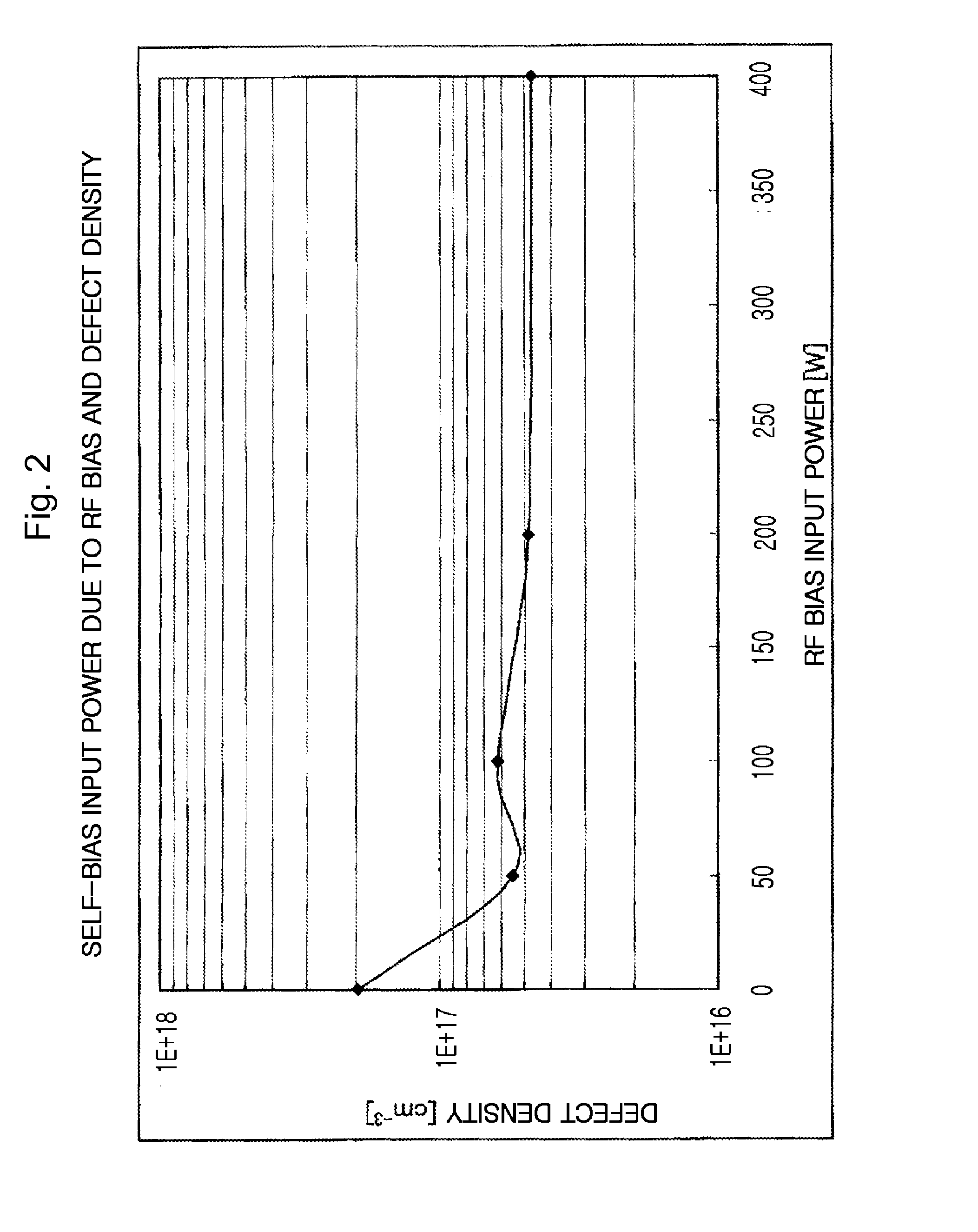
[0035]According to the present invention, in a process of supplying plasma excitation gas into a plasma excitation region formed above the substrate mounted on the base contained in a chamber, regulating pressure in the chamber, supplying raw gas into the chamber after introducing microwaves into the chamber, or introducing microwaves into the chamber after supplying raw gas into the chamber, and applying a
substrate bias voltage to the substrate, the bias
voltage functions as only a self-bias
voltage without varying the plasma. The bias power is adaptively selected in accordance with the type of gas. Thus,
irradiation ion energy on the surface of the substrate can be controlled.
[0036]In other words, by introducing the microwaves, high-density plasma is generated, and a film can be formed at a high speed by using the high-density plasma. Simultaneously, since
irradiation energy is controlled due to the
substrate bias voltage applied by the bias voltage application unit, a dense film can be formed, and thus, even when the film is exposed to the air,
oxygen is, to the maximum, prevented from mixing into the film, and thus a
low oxygen concentration is achieved. Accordingly a high-quality film in which defect density of the film is reduced can be formed.
[0037]Also, when this is applied to the field of the photoelectric conversion element, a high-quality Si film having a
low oxygen concentration and a lowered defect density can be formed so that reduction of dark
conductivity (leakage current) and improvement of
photoconductivity is promoted.
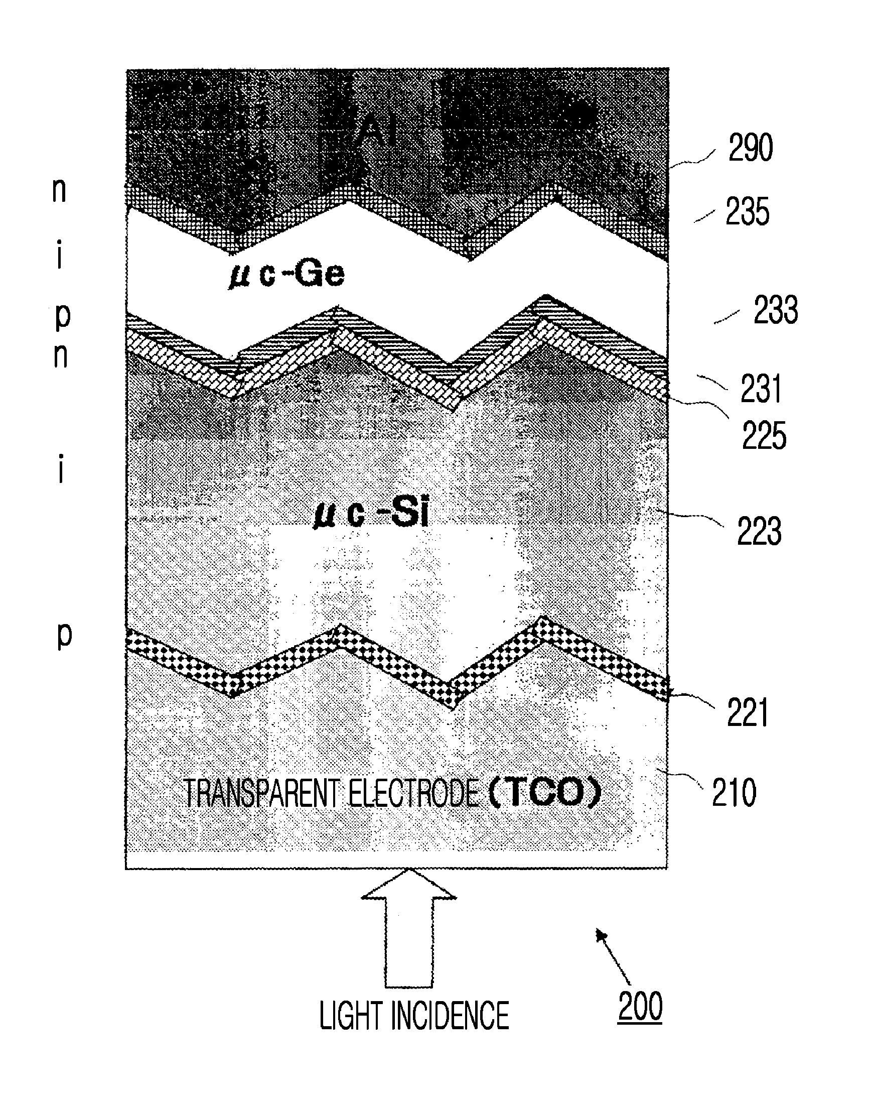
[0038]Also, in a tandem type
solar cell, two
layers are formed by stacking a first pin junction in which at least the i-layer including
microcrystalline or
polycrystalline silicon and a second pin junction in which at least the i-layer including
microcrystalline or polycrystalline
germanium so that a
solar cell in which efficient use of incident light and improvement of an optical absorption characteristic can be further promoted, can be manufactured.
[0039]Also, in the tandem type
solar cell, with respect to a first pin junction in which at least the i-layer including
amorphous silicon, a second pin junction in which at least the i-layer including
microcrystalline or
polycrystalline silicon germanium, and a third pin junction in which at least the i-layer including microcrystalline or polycrystalline
germanium, three
layers may be formed by stacking the
layers in the order of the first pin junction-second pin junction-third pin junction or the third pin junction-second pin junction-first pin junction, so that a solar
cell in which efficient use of incident light and improvement of an optical absorption characteristic can be further promoted, can be manufactured.
[0040]Also, in a film formation process of the tandem type solar
cell, by introducing microwaves, high-density plasma is generated, and a film can be formed at a high speed by using high-density plasma, and simultaneously,
irradiation energy is controlled by applying the substrate bias voltage so that a film can be densified. Accordingly, even when the film is exposed to the air,
oxygen is, to the maximum, prevented from mixing, and a oxygen concentration is lowered, and a high-quality film having a lowered defect density can be formed. In this regard, the solar
cell having superior characteristics, such as lowering of dark
conductivity (leakage current) and an increase of
photoconductivity, i.e., the solar cell having high conversion efficiency can be manufactured.

